没有合适的资源?快使用搜索试试~ 我知道了~
首页10Mbps/100Mbps/1000MbpsPCI以太网芯片说明书
10Mbps/100Mbps/1000MbpsPCI以太网芯片说明书
需积分: 48 12 下载量 148 浏览量
更新于2023-03-16
评论
收藏 830KB PDF 举报
DP83820 10/100/1000 Mb/s PCI Ethernet Network Interface Controller
资源详情
资源评论
资源推荐
DP83820
DP83820 10/100/1000 Mb/s PCI Ethernet Network Interface Controller
Literature Number: SNLS070B
DP83820 10/100/1000 Mb/s PCI Ethernet Network Interface Controller
© 2001 National Semiconductor Corporation
www.national.com
PRELIMINARY
February 2001
DP83820 10/100/1000 Mb/s PCI Ethernet Network Interface
Controller
General Description
DP83820 is a single-chip 10/100/1000 Mb/s Ethernet
Controller for the PCI bus. It is targeted at high-
performance adapter cards and mother boards. The
DP83820 fully implements the V2.2 66 MHz, 64-bit PCI bus
interface for host communications with power management
support. Packet descriptors and data are transferred via
bus-mastering, reducing the burden on the host CPU. The
DP83820 can support full duplex 10/100/1000 Mb/s
transmission and reception.
Features
— IEEE 802.3 Compliant, 66/33 Mhz, 64/32-bit PCI V2.2
MAC/BIU supports data rates from 1 Mb/s to 1000 Mb/s.
This allows support for traditional 10 Mb/s Ethernet, 100
Mb/s Fast Ethernet, as well as 1000 Mb/s Gigabit
Ethernet.
— Flexible, programmable Bus master - burst sizes of up to
256 dwords (1024 bytes)
— BIU compliant with PC 97 and PC 98 Hardware Design
Guides, PC 99 Hardware Design Guide draft, ACPI v1.0,
PCI Power Management Specification v1, OnNow
Device Class Power Management Reference
Specification - Network Device Class v1.0a
— Wake on LAN (WOL) support compliant with PC98,
PC99, and OnNow, including directed packets, Magic
Packet with SecureOn, ARP packets, pattern match
packets, and Phy status change
— GMII/MII provides IEEE 802.3 standard interface to
support 10/100/1000 Mb/s physical layer devices
— Ten-Bit Interface (TBI) for support of 1000BASE-X
— Virtual LAN (VLAN) and long frame support. VLAN tag
insertion support for transmit packets. VLAN tag
detection and removal for receive packets
— 802.3x Full duplex flow control, including automatic
transmission of Pause frames based on Rx FIFO
thresholds
— IPv.4 checksum task off-loading. Supports checksum
generation and verification of IP, TCP, and UDP headers
— 802.1D and 802.1Q priority queueing support. Supports
multiple priority queues in both transmit and receive
directions.
— Extremely flexible Rx packet filtration including: single
address perfect filter with MSb masking, broadcast,
2,048 entry multicast/unicast hash table, deep packet
pattern matching for up to 4 unique patterns.
— Statistics gathered for support of RFC 1213 (MIB II),
RFC 1398 (Ether-like MIB), IEEE 802.3 LME, reducing
CPU overhead for management.
— Internal 8 KB Transmit and 32 KB Receive data FIFOs
— Supports Jumbo packets
— Serial EEPROM port with auto-load of configuration data
from EEPROM at power-on
— Flash/PROM interface for remote boot support
— Full Duplex support for 10/100/1000 Mb/s data rates
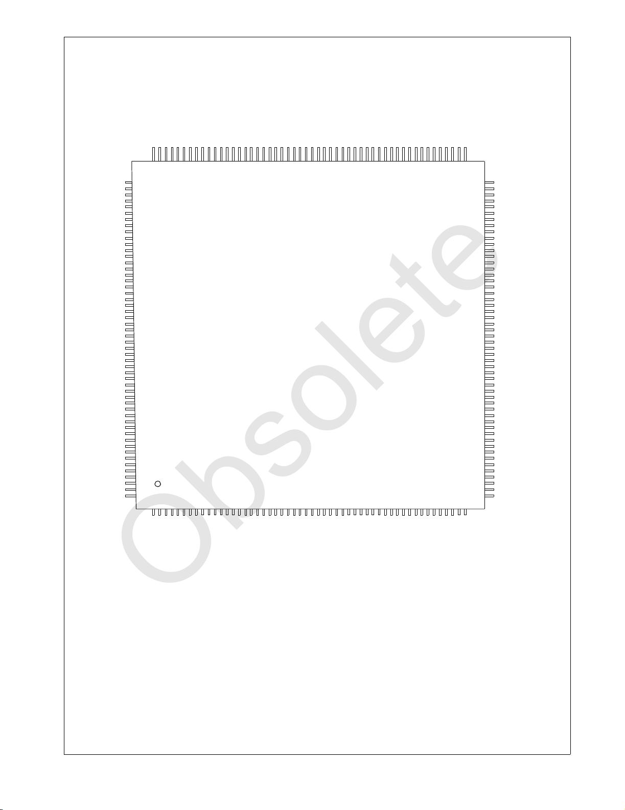
— 208-pin PQFP package
— Low power CMOS design
— 3.3V powered I/Os with 5V tolerant inputs
— JTAG Boundary Scan supported
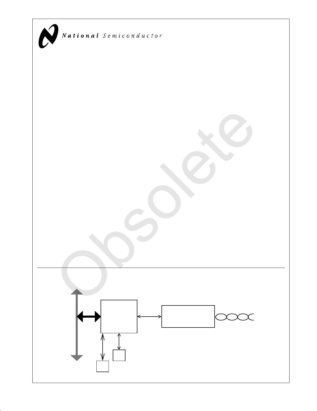
System Diagram
PCI Bus
DP83820
EEPROM (optional)
10/100/1000 Mb/s
PHY
Boot ROM (optional)
MII
GMII
Obsolete
2
www.national.com
1.0 Connection Diagram
Order Number DP83820VUW
See NS Package Number NVUW208A
AD16
CBEN2
PCIVSS
FRAMEN
IRDYN
TRDYN
PCIVDD
DEVSELN
STOPN
PERRN
SERRN
PAR
CBEN1
AD15
AD14
PCIVSS
AD13
AD12
AD11
PCIVDD
AD10
AD9
AD8
CBEN0
AD7
AD6
PCIVSS
AD5
AD4
PCIVDD
AD3
AD2
AD1
AD0
ACK64N
PCIVSS
REQ64N
CBEN7
CBEN6
PCIVDD
CBEN5
CBEN4
PAR64
AD63
AD62
PCIVSS
AD61
AD60
AD59
AD58
PCIVDD
AD57
MD7
MD6
MD5
MD4/EEDO
VDDIO
VSSIO
MD3
MD2
MD1/CFGDISN
MD0/PMGDISN
MWRN
MRDN
MCSN
EESEL
RESERVED
COREVDD
COREVSS
CLKRUNN
3VAUX
PWRGOOD
PCIVIO
AD32
AD33
AD34
PCIVDD
AD35
AD36
AD37
PCIVSS
AD38
AD39
AD40
AD41
PCIVDD
AD42
AD43
AD44
AD45
PCIVSS
AD46
AD47
AD48
AD49
AD50
PCIVDD
AD51
AD52
AD53
PCIVSS
AD54
AD55
AD56
RXD0
RXD1
RXD2
RXD3
VSSIO
VDDIO
RXD4
RXD5
RXD6
RXD7
RXDV/RXD8
RXER/RXD9
CRS/SIG_DET
COL
RXEN
PHYRSTN
COREVSS
COREVDD
PMEN
PCICLK
TRSTN
TCK
TMS
TDO
TDI
PCIVSS
INTAN
RSTN
GNTN
REQN
PCIVDD
AD31
AD30
AD29
AD28
AD27
AD26
AD25
AD24
PCIVSS
CBEN3
IDSEL
AD23
AD22
PCIVDD
AD21
AD20
AD19
COREVSS
COREVDD
AD18
AD17
157
158
159
160
161
162
163
164
165
166
167
168
169
170
171
172
173
174
175
176
177
178
179
180
181
182
183
184
185
186
187
188
189
190
191
192
193
194
195
196
197
198
199
200
201
202
203
204
205
206
207
208
1
2
3
4
5
6
7
8
9
10
11
12
13
14
15
16
17
18
19
20
21
22
23
24
25
26
27
28
29
30
31
32
33
34
35
36
37
38
39
40
41
42
43
44
45
46
47
48
49
50
51
52
104
103
102
101
100
99
98
97
96
95
94
93
92
91
90
89
88
87
86
85
84
83
82
81
80
79
78
77
76
75
74
73
72
71
70
69
68
67
66
65
64
63
62
61
60
59
58
57
56
55
54
53
156
155
154
153
152
151
150
149
148
147
146
145
144
143
142
141
140
139
138
137
136
135
134
133
132
131
130
129
128
127
126
125
124
123
122
121
120
119
118
117
116
115
114
113
112
111
110
109
108
107
106
105
DP83820
Gigabit NIC
RXCLK/RXPMACLK1
TXCLK/RXPMACLK0
TXER/TXD9
TXEN/TXD8
TXD7/MA15
TXD6/MA14
VDDIO
VSSIO
TXD5/MA13
TXD4/MA12
TXD3/MA11
TXD2/MA10
VDDIO
VSSIO
TXD1/MA9
TXD0/MA8
GTXCLK/TXPMACLK
MDIO
MDC
REF125
VDDIO
VSSIO
SPD1000
SPD100
PHYLNK
GP1DUP
GP5
GP4
GP3
GP2
RESERVED
AVDD
AVSS
OSCVDD
X1
X2
OSCVSS
RESERVED
RESERVED
RESERVED
COREVDD
COREVSS
MA7
MA6
MA5
VDDIO
VSSIO
MA4/EECLK
MA3/EEDI
MA2
MA1
MA0
Obsolete
3
www.national.com
2.0 Pin Descriptions
PCI Interface
Symbol Pin No(s) Direction Description
AD31-0 188, 189, 190,
191, 192, 193,
194, 195, 199,
200, 202, 203,
204, 207, 208,
1, 14, 15, 17,
18, 19, 21, 22,
23, 25, 26, 28,
29, 31, 32, 33,
34
I/O
Address and Data:
Multiplexed address and data bus. As a bus master, the
DP83820 will drive address during the first bus phase. During subsequent
phases, the DP83820 will either read or write data expecting the target to
increment its address pointer. As a bus target, the DP83820 will decode each
address on the bus and respond if it is the target being addressed.
CBEN3-0 197, 2, 13, 24 I/O
Bus Command/Byte Enable:
During the address phase these signals define
the “bus command” or the type of bus transaction that will take place. During the
data phase these pins indicate which byte lanes contain valid data. CBEN0
applies to byte 0 (bits 7-0) and CBEN3 applies to byte 3(bits 31-24).
PCICLK 176 I
Clock:
This PCI Bus clock provides timing for all bus phases. The rising edge
defines the start of each phase. The clock frequency ranges from 0 to 66 MHz.
DEVSELN 8 I/O
Device Select:
As a target, the DP83820 asserts this signal low when it
recognizes its address after FRAMEN is asserted. As a bus master, the
DP83820 samples this signal to insure that the destination address for the data
transfer is recognized by a PCI target.
FRAMEN 4 I/O
Frame:
As a bus master, this signal is asserted low to indicate the beginning
and duration of a bus transaction. Data transfer takes place when this signal is
asserted. It is de-asserted before the transaction is in its final phase. As a
target, the device monitors this signal before decoding the address to check if
the current transaction is addressed to it.
GNTN 185 I
Grant:
This signal is asserted low to indicate to the DP83820 that it has been
granted ownership of the bus by the central arbiter. This input is used when the
DP83820 is acting as a bus master.
IDSEL 198 I
Initialization Device Select:
This pin is sampled by the DP83820 to identify
when configuration read and write accesses are intended for it.
INTAN 183 O
Interrupt A:
This signal is asserted low when an interrupt condition as defined
in the Interrupt Status Register, Interrupt Mask, and Interrupt Enable registers
occurs.
IRDYN 5 I/O
Initiator Ready:
As a bus master, this signal will be asserted low when the
DP83820 is ready to complete the current data phase transaction. This signal is
used in conjunction with the TRYDN signal. Data transaction takes place at the
rising edge of PCICLK when both IRDYN and TRDYN are asserted low. As a
target, this signal indicates that the master has put the data on the bus.
PAR 12 I/O
Parity:
This signal indicates even parity across AD31-0 and CBEN3-0 including
the PAR pin. As a master, PAR is asserted during address and write data
phases. As a target, PAR is asserted during read data phases.
PERRN 10 I/O
Parity Error:
The DP83820 as a master or target will assert this signal low to
indicate a parity error on any incoming data (except for special cycles). As a bus
master, it will monitor this signal on all write operations (except for special
cycles).
REQN 186 O
Request:
The DP83820 will assert this signal low to request the ownership of
the bus to the central arbiter.
RSTN 184 I
Reset:
When this signal is asserted all outputs of DP83820 will be tri-stated
and the device will be put into a known state.
Obsolete
4
www.national.com
2.0 Pin Descriptions
(Continued)
SERRN 11 I/O
System Error:
This signal is asserted low by DP83820 during address parity
errors and system errors if enabled.
STOPN 9 I/O
Stop:
This signal is asserted low by the target device to request the master
device to stop the current transaction.
TRDYN 6 I/O
Target Ready:
As a target, this signal will be asserted low when the (slave)
device is ready to complete the current data phase transaction. This signal is
used in conjunction with the IRDYN signal. Data transaction takes place at the
rising edge of PCICLK when both IRDYN and TRDYN are asserted low. As a
master, this signal indicates that the target is ready for the data during write
operation and with the data during read operation.
PMEN 175 O
Power Management Event:
This signal is asserted low by DP83820 to indicate
that a power management event has occurred.
3VAUX 86 I
PCI Aux Voltage Sense:
This pin is used to sense the presence of a 3.3v
auxiliary supply in order to define the PME Support available.
This pin pad has an internal weak pull down.
PWRGOOD 85 I
PCI bus power good:
Connected to PCI bus 3.3v power, this pin is used to
sense the presence of PCI bus power during the D3 power management state.
This pin pad has an internal weak pull down.
CLKRUNN 87 I/O
Clockrun
: This signal is asserted low by DP83820 to indicate that a Clockrun
Event has occurred.
AD63-32 44, 45, 47, 48,
49, 50, 52, 53,
54, 55, 57, 58,
59, 61, 62, 63,
64, 65, 67, 68,
69, 70, 72, 73,
74, 75, 77, 78,
79, 81, 82, 83
I/O
64-bit Extension Address and Data:
Multiplexed address and data bus.
Provides upper address bits during 64-bit DAC command. During data phase,
used for transferring upper 32-bits of a 64-bit data transaction.
CBEN7-4 38, 39, 41, 42 I/O
64-bit Extension Bus Command/Byte Enables:
During the address phase
these signals define the “bus command” for a 64-bit DAC command. During a
64-bit data phase these pins indicate which byte lanes contain valid data.
CBEN4 applies to byte 4(bits 39-32) and CBEN7 applies to byte 7(bits 63-56).
REQ64N 37 I/O
Request 64-bit Transfer:
The DP83820 will assert this signal low to request a
64-bit transfer of data. This pin is sampled by the DP83820 during reset to
determine if the device is connected to a 64-bit datapath.
ACK64N 35 I
Acknowledge 64-bit Transfer:
The DP83820 will samples this signal on bus
master cycles when it has requested a 64-bit data transfer. If both REQ64N and
ACK64N are asserted, then a 64-bit transfer will be performed. As a target, the
DP83820 only supports 32-bit transfers, so it will never assert ACK64N.
PAR64 43 I/O
Parity Upper DWORD:
This signal indicates even parity across AD63-32 and
CBEN7-4 including the PAR64 pin. As a master, PAR64 is driven during
address and write data phases. As a target, the DP83820 only supports 32-bit
transfers, so it will not drive PAR64.
PCIVIO 84 I
PCI Bus VIO:
This pin should be connected to the VIO pins of the PCI bus. It
provides a direct connection to the ESDPLUS ring for biasing. It may be
connected to 5V if available. It should not be connected to 3.3V unless all
signaling is 3.3V as this will interfere with 5V tolerance. Care should be taken in
connecting this to power supplies when power management functions are
enabled.
PCI Interface
Symbol Pin No(s) Direction Description
Obsolete
剩余88页未读,继续阅读
danny63
- 粉丝: 1
- 资源: 10
上传资源 快速赚钱
- 我的内容管理 收起
- 我的资源 快来上传第一个资源
- 我的收益 登录查看自己的收益
- 我的积分 登录查看自己的积分
- 我的C币 登录后查看C币余额
- 我的收藏
- 我的下载
- 下载帮助
会员权益专享
最新资源
- 27页智慧街道信息化建设综合解决方案.pptx
- 计算机二级Ms-Office选择题汇总.doc
- 单链表的插入和删除实验报告 (2).docx
- 单链表的插入和删除实验报告.pdf
- 物联网智能终端项目设备管理方案.pdf
- 如何打造品牌的模式.doc
- 样式控制与页面布局.pdf
- 武汉理工Java实验报告(二).docx
- 2021线上新品消费趋势报告.pdf
- 第3章 Matlab中的矩阵及其运算.docx
- 基于Web的人力资源管理系统的必要性和可行性.doc
- 基于一阶倒立摆的matlab仿真实验.doc
- 速运公司物流管理模式研究教材
- 大数据与管理.pptx
- 单片机课程设计之步进电机.doc
- 大数据与数据挖掘.pptx
资源上传下载、课程学习等过程中有任何疑问或建议,欢迎提出宝贵意见哦~我们会及时处理!
点击此处反馈
安全验证
文档复制为VIP权益,开通VIP直接复制
信息提交成功
评论0