
ANTC206
Differential Clock Translation
Introduction
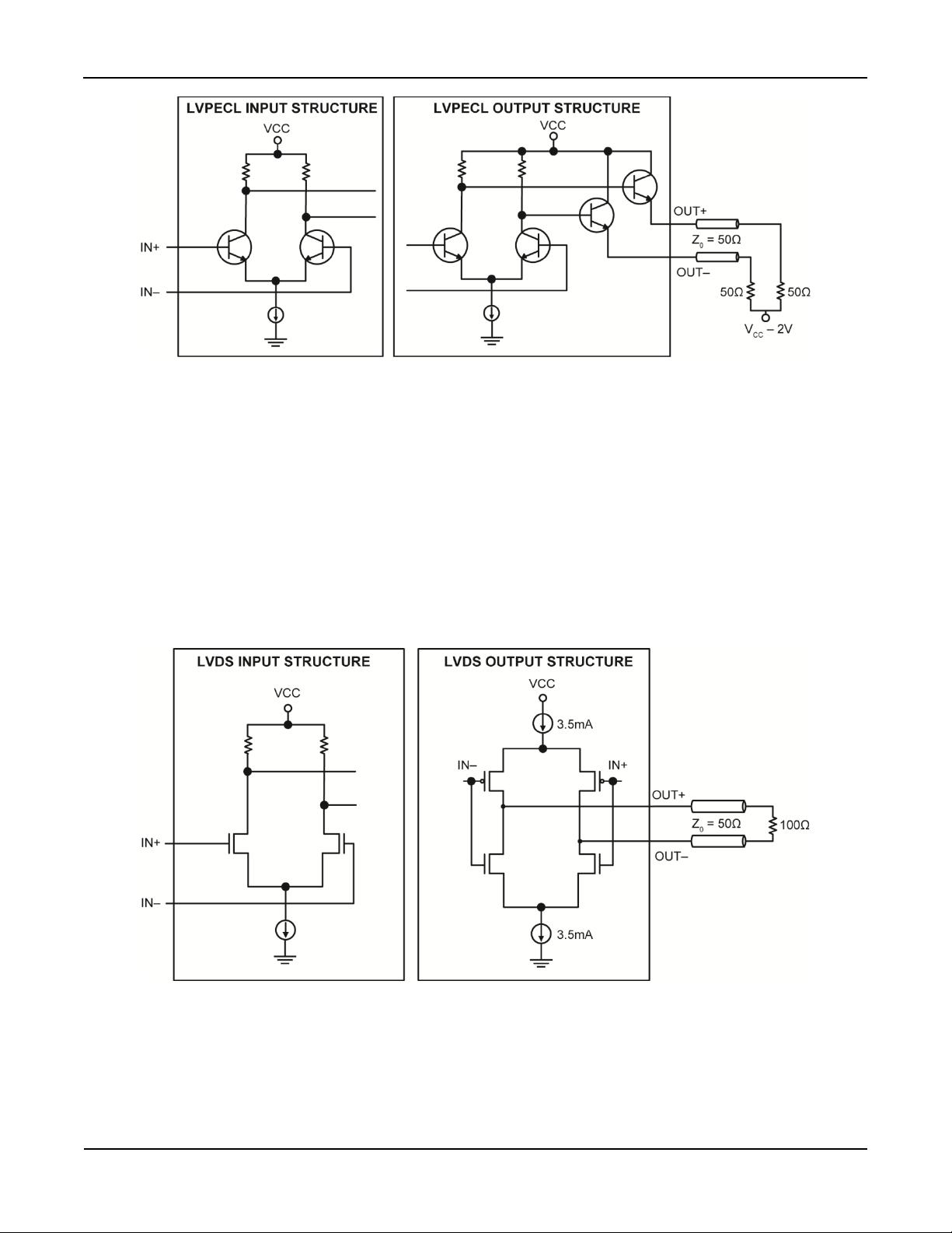
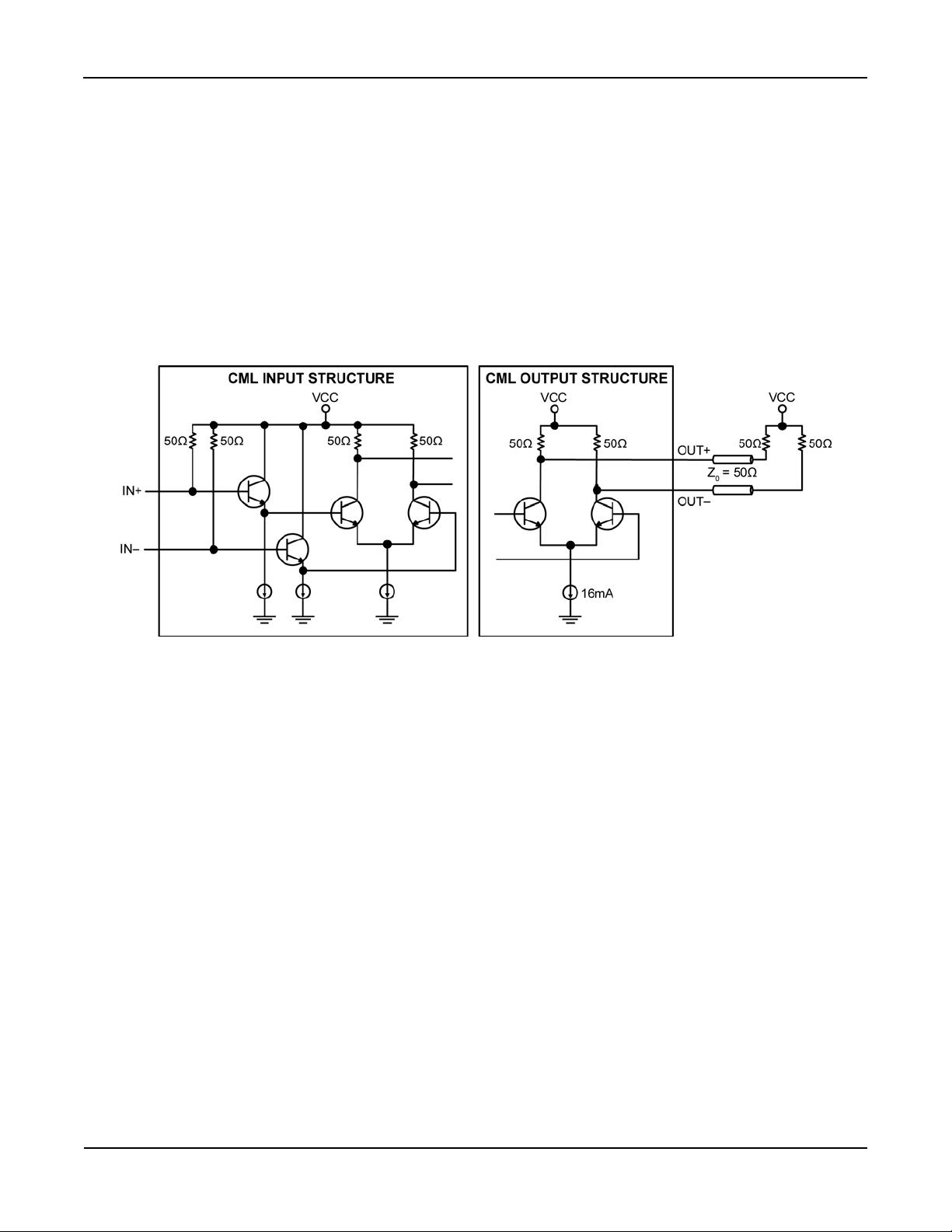
Considering that each available clock logic type (LVPECL, HCSL, CML, and LVDS) operates with a different
common-mode voltage and swing level than the next (see Table 1), it is necessary to design clock logic
translation between the driver side and receiver side for any given system design. This application note details
how to translate one differential clock into other types of differential logics by adding attenuation resistors and bias
circuits between them to attenuate the swing level and re-bias the common-mode for the input of the receiver.
Table 1. Common-Mode Voltage and Swing Levels of Different Clock Logic Types
Specification LVPECL LVDS CML Terminated 50Ω to V
CC
HCSL
V
CM
V
CC
− 1.4V
1.2V
V
CC
− 0.2V
350mV
V
SWING_SE
800mV 325mV 400mV 700mV
V
OH
V
CC
− 1V
1.3625V V
CC
700mV
V
OL
V
CC
− 1.8V
1.0375V
V
CC
− 0.400V
0V
Reference V
CC
Ground V
CC
Ground
Input/Output Structure of Each Differential Clock Logic
Prior to designing the logic translation circuit, an examination of the input/output structures of each logic type −
LVPECL, HCSL, CML, and LVDS − is required as each logic type features a different common-mode voltage and
swing level.
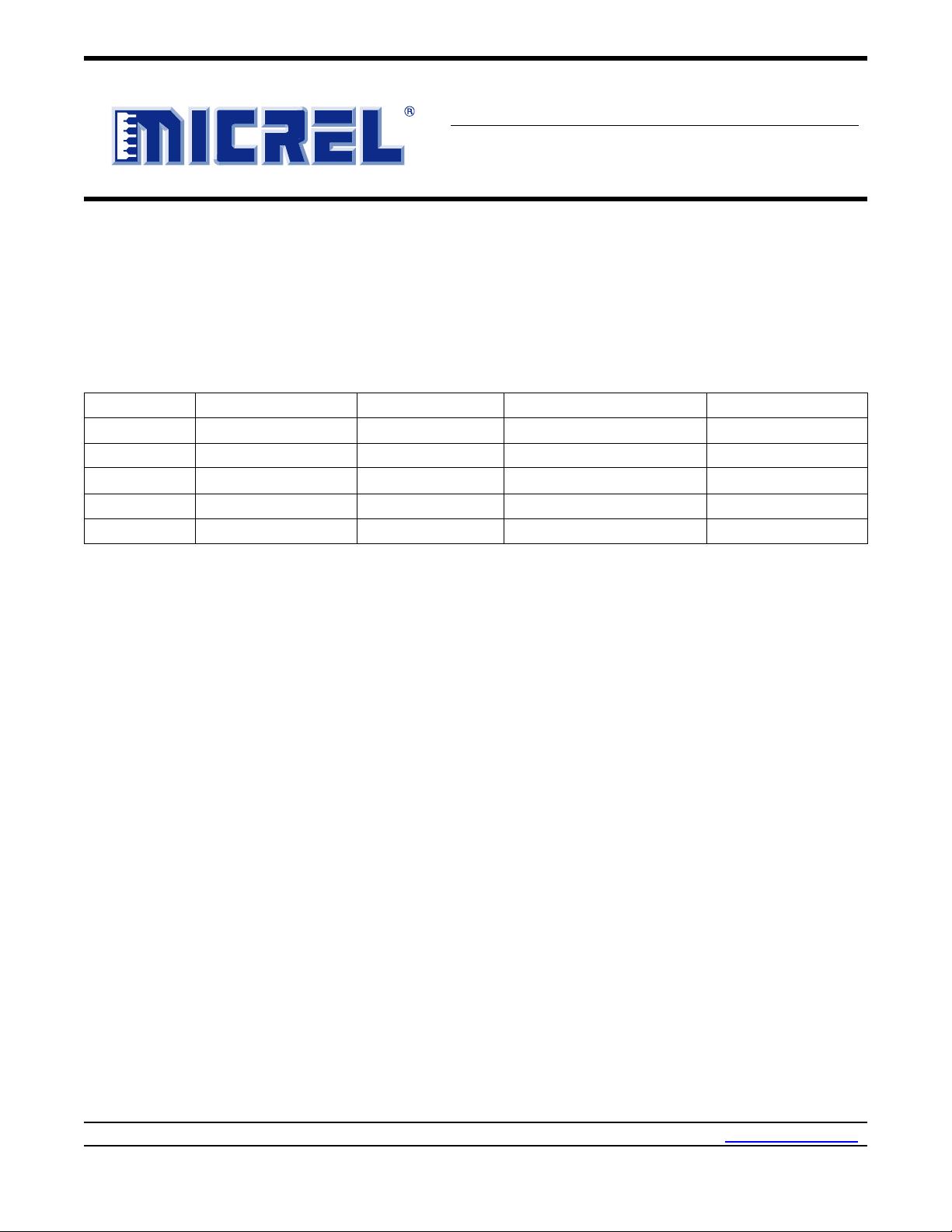
Low-Voltage, Positive-Referenced, Emitter-Coupled Logic (LVPECL)
Low-voltage, positive-referenced, emitter-coupled logic (LVPECL) originates from emitter-coupled logic (ECL),
adopting a positive power supply.
The LVPECL input is a current-switching differential pair with high input impedance (see Figure 1). The input
common-mode voltage should be approximately V
CC
− 1.3V for the purpose of having operating headroom, either
from internal self-biasing or external biasing.
The LVPECL output consists of a differential pair amplifier which drives a pair of emitter followers (or open
emitters) as illustrated in Figure 1. The output emitter followers should operate in the “active” region with DC
current at all times. The output pins of OUT+ and OUT− are typically connected to differential transmission lines
(Z
0
= 100Ω) or a single-ended transmission line (Z
0
= 50Ω) for impedance matching. The proper termination for
LVPECL output is 50Ω to V
CC
− 2V and OUT+/OUT− will typically be V
CC
− 1.3V, resulting in an approximate DC
current flow of 14mA.
Another way to terminate LVPECL output is to apply 142Ω to GND, which provides a DC-biasing for LVPECL
output and a DC current path to GND. Because the LVPECL output common-mode is at V
CC
− 1.3V, the DC-
biasing resistor can be selected by assuming a DC current of 14mA (R = V
CC
− 1.3V / 14mA), resulting in R =
142Ω (150Ω also works) for V
CC
− 3.3V.
Micrel Inc. • 2180 Fortune Drive • San Jose, CA 95131 • USA • tel +1 (408) 944-0800 • fax + 1 (408) 474-1000 • http://www.micrel.com
July 9, 2014
Revision 1.0
Edited by Foxit Reader
Copyright(C) by Foxit Software Company,2005-2008
For Evaluation Only.
剩余11页未读,继续阅读

wscsyyych
- 粉丝: 4
- 资源: 8
 我的内容管理
收起
我的内容管理
收起
- 我的资源
快来上传第一个资源
 我的收益 登录查看自己的收益
 我的积分
登录查看自己的积分
我的积分
登录查看自己的积分
 我的C币
登录后查看C币余额
我的C币
登录后查看C币余额
 我的收藏
我的收藏  我的下载
我的下载  下载帮助
下载帮助

会员权益专享


最新资源
- c++校园超市商品信息管理系统课程设计说明书(含源代码) (2).pdf
- 建筑供配电系统相关课件.pptx
- 企业管理规章制度及管理模式.doc
- vb打开摄像头.doc
- 云计算-可信计算中认证协议改进方案.pdf
- [详细完整版]单片机编程4.ppt
- c语言常用算法.pdf
- c++经典程序代码大全.pdf
- 单片机数字时钟资料.doc
- 11项目管理前沿1.0.pptx
- 基于ssm的“魅力”繁峙宣传网站的设计与实现论文.doc
- 智慧交通综合解决方案.pptx
- 建筑防潮设计-PowerPointPresentati.pptx
- SPC统计过程控制程序.pptx
- SPC统计方法基础知识.pptx
- MW全能培训汽轮机调节保安系统PPT教学课件.pptx
资源上传下载、课程学习等过程中有任何疑问或建议,欢迎提出宝贵意见哦~我们会及时处理!
点击此处反馈


评论2