没有合适的资源?快使用搜索试试~ 我知道了~
首页HT16C23完全替代兼容VK2C23 /LCD液晶驱动,pdf中文资料,引脚图,电路,设计指南
VK2C23 是一款存储器映射和多功能 的 LCD 控制 / 驱动芯片。该芯片的显示字段为 224 点 (56 SEG × 4 COM) 或 416 点 (52 SEG × 8 COM)。VK2C23 芯片的软件配置特 性使其适用于多种 LCD 应用,包括 LCD 模块和 显示子系统。VK2C23 芯片可通过双 线双向 I2C 接口与大多数微处理器或微控制器进 行通信。
资源详情
资源评论
资源推荐
Rev. 1.20 1 November 07 , 2017 Rev. 1.00 PB January 27, 2015
VK2C23 56
×
4 / 52
×
8 LCD Driver Controller
Features
• Operating voltage: 2.4 ~ 5.5V
• Internal 32kHz RC oscillator
• Bias: 1/3 or 1/4; Duty:1/4 or 1/8
• Internal LCD bias generation with voltage-follower
buffers
• I
2
C-bus interface
• Two Selectable LCD frame frequencies: 80Hz or
160Hz
•
•
Up to 52 x 8 bits RAM for display data storage
Display patterns:
– 56 x 4 patterns: 56 segments and 4 commons
– 52 x 8 patterns: 52 segments and 8 commons
• Versatile blinking modes
• R/W address auto increment
• Internal 16-step voltage adjustment to adjust LCD
operating voltage
• Low power consumption
• Provides V
LCD
pin to adjust LCD operating voltage
• Manufactured in silicon gate CMOS process
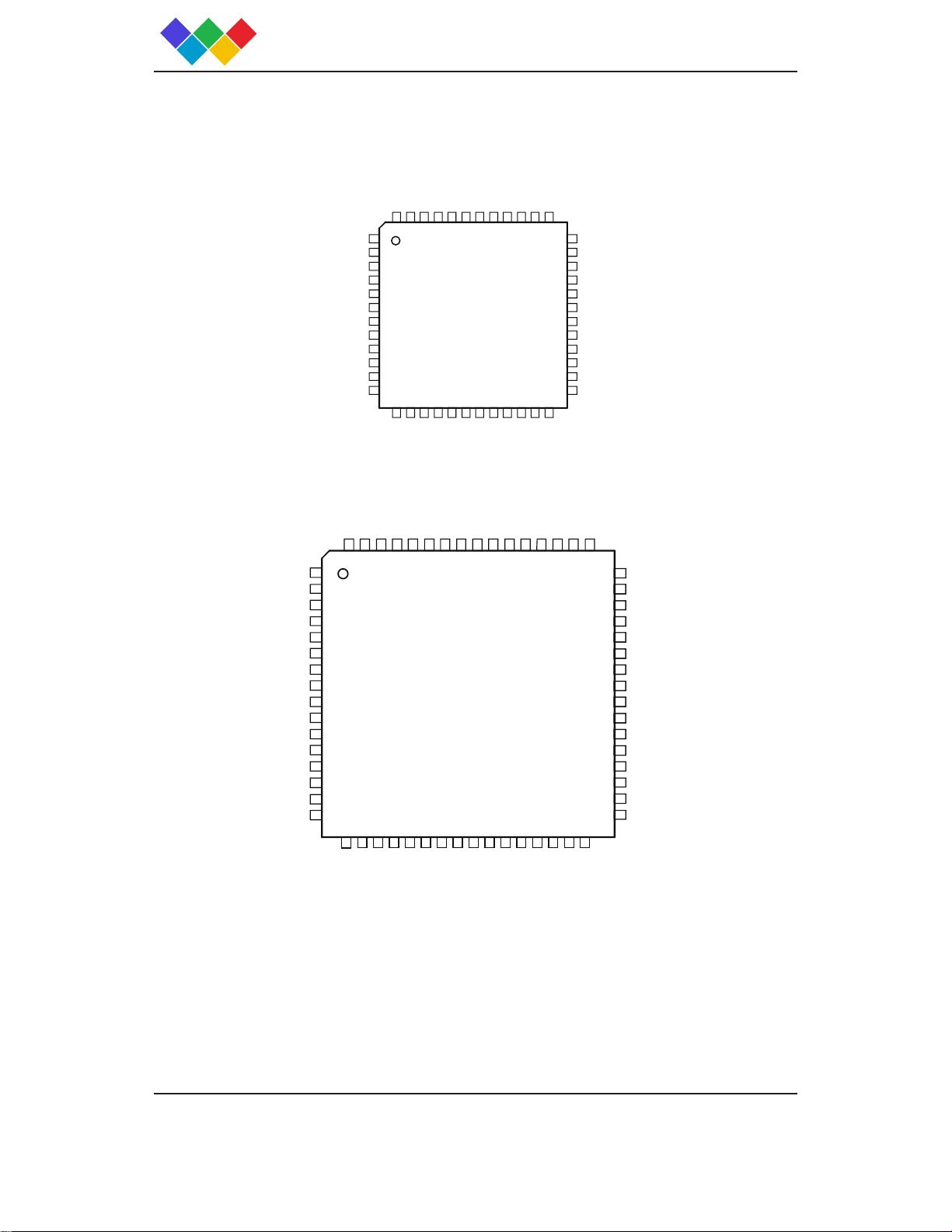
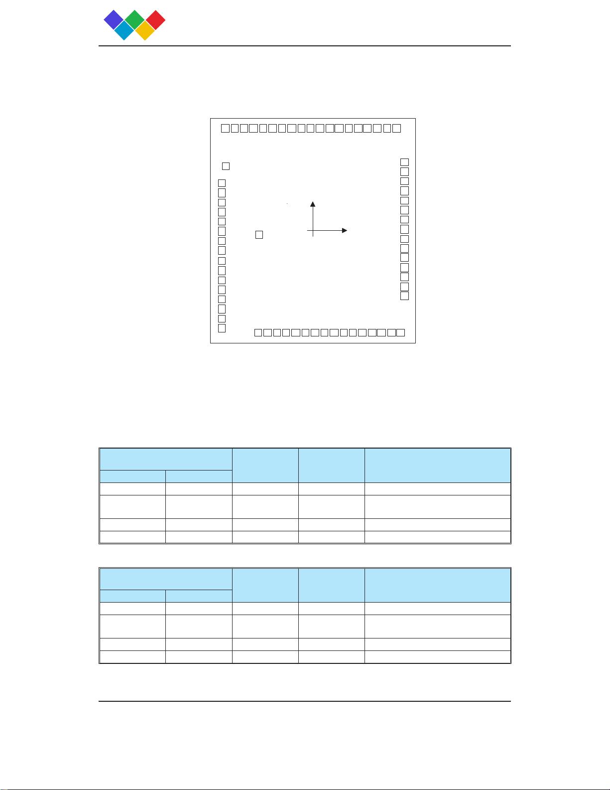
• Package Type: 48LQFP, 64LQFP, Chip and
Goldbump chip.
Applications
• Electronic meter
• Water meter
• Gas meter
• Heat energy meter
General Description
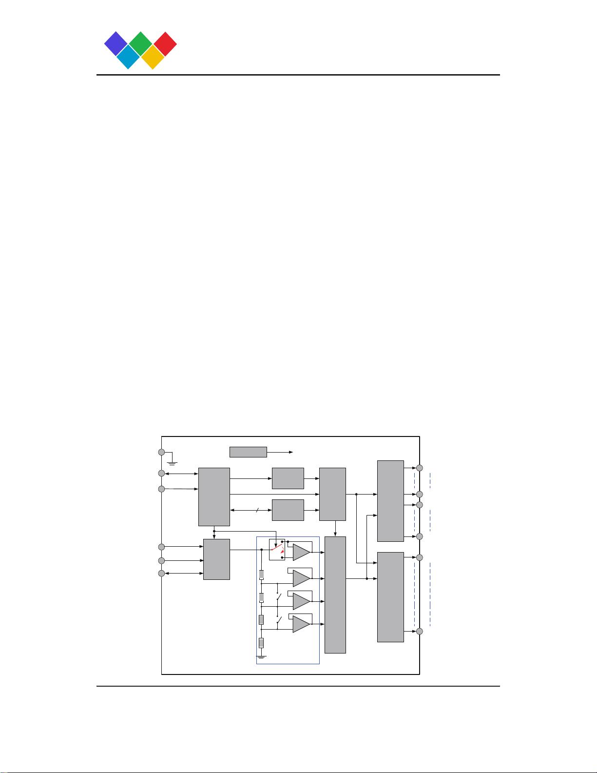
The VK2C23 device is a memory mapping and multi-function
LCD controller driver. The Display
segments of the device are 224 patterns (56 segments and 4commons) or 416 patterns (52 segments and
8commons). The software configuration feature of the VK2C23 device makes it suitable for multiple LCD
applications including LCD modules and display subsystems. The VK2C23 device communicates
with most microprocessors / microcontrollers via a two-line bidirectional I
2
C-bus.
Block Diagram
LCD
Voltage
Selector
Column
/Segment
driver
output
Segment
driver
output
Display RAM
52*8bits
Timing
generator
I2C
Controller
COM0
COM3
SEG4
VLCD
VSS
SDA
SCL
Internal RC
Oscillator
Power_on reset
R
-
+
OP1
COM4/SEG0
COM7/SEG3
R
-
+
OP2
SEG55
VDD
LCD bias generator
R
8
R
-
+
OP3
Internal
voltage
adjustment
-
+
OP4
VCCA2
•Household appliance
•Games
•Telephone
•Consumer electronics
深圳市永嘉微电科技有限公司
www.szvinka.com/
Rev. 1.20 2 November 07 , 2017
VK2C23 56×4 / 52×8 LCD Driver Controller
Pin Assignment
1
2
3
4
5
6
7
8
9
10
11
12
13 14 1516 17 18 19 20 2122 23 24
25
26
27
28
29
30
31
32
33
34
35
36
45464748
3738394041424344
VK2C23 B
48 LQFP-A
SEG27
SEG26
SEG25
SEG24
SEG23
SEG22
SEG21
SEG20
SEG19
SEG18
SEG17
SEG16
VDD
SDA
SCL
VSS
COM0
COM1
COM2
COM3
COM4
COM5
COM6
COM7
SEG15
SEG14
SEG13
SEG12
SEG11
SEG10
SEG9
SEG8
SEG7
SEG6
SEG5
SEG4
SEG28
SEG29
SEG30
SEG31
SEG32
SEG33
SEG34
SEG35
SEG36
SEG37
SEG38
VLCD
HT16C23
64 LQFP-A
SEG39
SEG38
SEG37
SEG36
SEG35
SEG34
SEG33
SEG32
SEG31
SEG30
SEG29
SEG28
SEG27
SEG26
SEG25
SEG24
VDD
SDA
SCL
VSS
COM0
COM1
COM2
COM3
COM4/SEG0
COM5/SEG1
COM6/SEG2
COM7/SEG3
SEG4
SEG5
SEG6
SEG7
17 18 19 20 21 22 23 24 25 26 27 28 29 30 31 32
64 63 62 61 60 59 58 57 56 55 54 53 52 51 50 49
1
2
3
4
5
6
7
8
9
10
11
12
13
14
15
16
48
47
46
45
44
43
42
41
40
39
38
37
36
35
34
33
SEG23
SEG22
SEG21
SEG20
SEG19
SEG18
SEG17
SEG16
SEG15
SEG14
SEG13
SEG12
SEG11
SEG10
SEG9
SEG8
SEG40
SEG41
SEG42
SEG43
SEG44
SEG45
SEG46
SEG47
SEG48
SEG49
SEG50
SEG51
SEG52
SEG53
SEG54
VLCD
1
2
3
4
5
6
7
8
9
10
11
12
13 14 1516 17 18 19 20 2122 23 24
25
26
27
28
29
30
31
32
33
34
35
36
45464748
3738394041424344
HT16C23
48 LQFP-A
SEG27
SEG26
SEG25
SEG24
SEG23
SEG22
SEG21
SEG20
SEG19
SEG18
SEG17
SEG16
VDD
SDA
SCL
VSS
COM0
COM1
COM2
COM3
COM4
COM5
COM6
COM7
SEG15
SEG14
SEG13
SEG12
SEG11
SEG10
SEG9
SEG8
SEG7
SEG6
SEG5
SEG4
SEG28
SEG29
SEG30
SEG31
SEG32
SEG33
SEG34
SEG35
SEG36
SEG37
SEG38
SEG39
HT16C23
64 LQFP-A
SEG39
SEG38
SEG37
SEG36
SEG35
SEG34
SEG33
SEG32
SEG31
SEG30
SEG29
SEG28
SEG27
SEG26
SEG25
SEG24
VDD
SDA
SCL
VSS
COM0
COM1
COM2
COM3
COM4/SEG0
COM5/SEG1
COM6/SEG2
COM7/SEG3
SEG4
SEG5
SEG6
SEG7
17 18 19 20 21 22 23 24 25 26 27 28 29 30 31 32
64 63 62 61 60 59 58 57 56 55 54 53 52 51 50 49
1
2
3
4
5
6
7
8
9
10
11
12
13
14
15
16
48
47
46
45
44
43
42
41
40
39
38
37
36
35
34
33
SEG23
SEG22
SEG21
SEG20
SEG19
SEG18
SEG17
SEG16
SEG15
SEG14
SEG13
SEG12
SEG11
SEG10
SEG9
SEG8
SEG40
SEG41
SEG42
SEG43
SEG44
SEG45
SEG46
SEG47
SEG48
SEG49
SEG50
SEG51
SEG52
SEG53
SEG54
SEG55
1
2
3
4
5
6
7
8
9
10
11
12
13 14 1516 17 18 19 20 2122 23 24
25
26
27
28
29
30
31
32
33
34
35
36
45464748
3738394041424344
HT16C23
48 LQFP-A
SEG27
SEG26
SEG25
SEG24
SEG23
SEG22
SEG21
SEG20
SEG19
SEG18
SEG17
SEG16
VDD
SDA
SCL
VSS
COM0
COM1
COM2
COM3
COM4
COM5
COM6
COM7
SEG15
SEG14
SEG13
SEG12
SEG11
SEG10
SEG9
SEG8
SEG7
SEG6
SEG5
SEG4
SEG28
SEG29
SEG30
SEG31
SEG32
SEG33
SEG34
SEG35
SEG36
SEG37
SEG38
VLCD
VK2C23 A
64 LQFP-A
SEG39
SEG38
SEG37
SEG36
SEG35
SEG34
SEG33
SEG32
SEG31
SEG30
SEG29
SEG28
SEG27
SEG26
SEG25
SEG24
VDD
SDA
SCL
VSS
COM0
COM1
COM2
COM3
COM4/SEG0
COM5/SEG1
COM6/SEG2
COM7/SEG3
SEG4
SEG5
SEG6
SEG7
17 18 19 20 21 22 23 24 25 26 27 28 29 30 31 32
64 63 62 61 60 59 58 57 56 55 54 53 52 51 50 49
1
2
3
4
5
6
7
8
9
10
11
12
13
14
15
16
48
47
46
45
44
43
42
41
40
39
38
37
36
35
34
33
SEG23
SEG22
SEG21
SEG20
SEG19
SEG18
SEG17
SEG16
SEG15
SEG14
SEG13
SEG12
SEG11
SEG10
SEG9
SEG8
SEG40
SEG41
SEG42
SEG43
SEG44
SEG45
SEG46
SEG47
SEG48
SEG49
SEG50
SEG51
SEG52
SEG53
SEG54
VLCD
1
2
3
4
5
6
7
8
9
10
11
12
13 14 1516 17 18 19 20 2122 23 24
25
26
27
28
29
30
31
32
33
34
35
36
45464748
3738394041424344
HT16C23
48 LQFP-A
SEG27
SEG26
SEG25
SEG24
SEG23
SEG22
SEG21
SEG20
SEG19
SEG18
SEG17
SEG16
VDD
SDA
SCL
VSS
COM0
COM1
COM2
COM3
COM4
COM5
COM6
COM7
SEG15
SEG14
SEG13
SEG12
SEG11
SEG10
SEG9
SEG8
SEG7
SEG6
SEG5
SEG4
SEG28
SEG29
SEG30
SEG31
SEG32
SEG33
SEG34
SEG35
SEG36
SEG37
SEG38
SEG39
HT16C23
64 LQFP-A
SEG39
SEG38
SEG37
SEG36
SEG35
SEG34
SEG33
SEG32
SEG31
SEG30
SEG29
SEG28
SEG27
SEG26
SEG25
SEG24
VDD
SDA
SCL
VSS
COM0
COM1
COM2
COM3
COM4/SEG0
COM5/SEG1
COM6/SEG2
COM7/SEG3
SEG4
SEG5
SEG6
SEG7
17 18 19 20 21 22 23 24 25 26 27 28 29 30 31 32
64 63 62 61 60 59 58 57 56 55 54 53 52 51 50 49
1
2
3
4
5
6
7
8
9
10
11
12
13
14
15
16
48
47
46
45
44
43
42
41
40
39
38
37
36
35
34
33
SEG23
SEG22
SEG21
SEG20
SEG19
SEG18
SEG17
SEG16
SEG15
SEG14
SEG13
SEG12
SEG11
SEG10
SEG9
SEG8
SEG40
SEG41
SEG42
SEG43
SEG44
SEG45
SEG46
SEG47
SEG48
SEG49
SEG50
SEG51
SEG52
SEG53
SEG54
SEG55
Note: 1. Application at V
DD
≤ V
LCD
or V
LCD
≤ V
DD
.
2. When the 48-pin LQFP package is selected, this device does not support LCD 1/4 duty.
3. The VCCA2 pad is internally connected with the VLCD pad.
深圳市永嘉微电科技有限公司
www.szvinka.com/
Rev. 1.20 3 November 07 , 2017
Pad assignment for COB
(0, 0)
22 3534333230 3129282726252423
50
1
SDA
SCL
Option
VSS
COM0
COM1
COM2
COM3
COM4/SEG0
COM5/SEG1
COM6/SEG2
COM7/SEG3
SEG4
SEG5
SEG6
SEG7
SEG38
SEG37
SEG36
SEG35
SEG34
SEG33
SEG32
SEG31
SEG30
SEG29
SEG28
SEG27
SEG26
SEG25
SEG24
SEG39
SEG40
SEG41
SEG42
SEG43
SEG44
SEG45
SEG46
SEG47
SEG48
SEG49
SEG50
SEG51
SEG52
SEG53
SEG54
SEG55
VLCD
VCCA2
SEG23
SEG22
SEG21
SEG20
SEG19
SEG18
SEG17
SEG16
SEG15
SEG14
SEG13
SEG12
SEG11
SEG10
SEG9
SEG8
VDD
N.C.
68 67 66 65 64 63 62 61 5859 57 56 55 54 53 52 5160
36
49
48
47
46
45
44
43
42
41
40
39
38
37
2
3
4
6
5
7
8
10
9
11
12
13
14
15
16
17
18
19
20 21
Chip size: 1843 x 2018μm
2
Note: 1. The option (pad 5) must be bonded to V
DD
or oating.
2. The IC substrate should be connected to V
SS
in the PCB layout artwork.
3. VLCD (pad 68) and VCCA2 (pad 1) must be bonded together for the application at V
DD
≤ V
LCD
or
V
LCD
≤ V
DD
.
Internal voltage adjustment (IVA)
set command
VLCD
(pad 68)
SEG55
(pad 67)
Note
DE bit VE bit
0 0 Input Null
● VLCD support internal bias voltage.
0 1 Input Null
● Internal Voltage Adjustment is null
● VLCD support internal bias voltage
1 0 Input Output
● VLCD support internal bias voltage
1 1 Input Output
● VLCD support internal bias voltage
4. VDD (pad2) and VCCA2 (pad 1) must be bonded together for the application at V
LCD
≤
V
DD
.
Internal voltage adjustment (IVA)
set command
VLCD
(pad 68)
SEG55
(pad 67)
Note
DE bit VE bit
0 0 Input Null
● VLCD support internal bias voltage.
0 1 Output Null
● Detect the internal bias voltage
● VDD support internal bias voltage
1 0 Floating Output
● VDD support internal bias voltage
1 1 Floating Output
● VDD support internal bias voltage
VK2C23 56×4 / 52×8 LCD Driver Controller
深圳市永嘉微电科技有限公司
www.szvinka.com/
Rev. 1.20 4 November 07 , 2017
Pad Coordinates for COB
Unit: μm
No Name X Y No Name X Y
1 VCCA2 -788.05 905.4 35 SEG23 780.15 -905.4
2 VDD -783.15 572.25 36 SEG24 817.45 -582.35
3 SDA -817.9 419.55 37 SEG25 817.45 -497.35
4 SCL -817.9 334.55 38 SEG26 817.45 -412.35
5 OPTION -817.9 249.55 39 SEG27 817.45 -327.35
6 VSS -817.9 164.55 40 SEG28 817.45 -242.35
7 COM0 -817.9 79.55 41 SEG29 817.45 -157.35
8 COM1 -817.9 -5.45 42 SEG30 817.45 -72.35
9 N.C. -484.014 -35.6 43 SEG31 817.45 12.65
10 COM2 -817.9 -90.45 44 SEG32 817.45 97.65
11 COM3 -817.9 -175.45 45 SEG33 817.45 182.65
12 COM4/SEG0 -817.9 -270.35 46 SEG34 817.45 267.65
13 COM5/SEG1 -817.9 -355.35 47 SEG35 817.45 352.65
14 COM6/SEG2 -817.9 -440.35 48 SEG36 817.45 437.65
15 COM7/SEG3 -817.9 -525.35 49 SEG37 817.45 522.65
16 SEG4 -817.9 -613.1 50 SEG38
817.45 607.65
17 SEG5 -817.9 -698.1 51 SEG39 741.95 905.4
18 SEG6 -817.9 -783.1 52 SEG40 656.95 905.4
19 SEG7 -817.9 -868.1 53 SEG41 571.95 905.4
20 SEG8 -494.85 -905.4 54 SEG42 486.95 905.4
21 SEG9 -409.85 -905.4 55 SEG43 401.95 905.4
22 SEG10 -324.85 -905.4 56 SEG44 316.95 905.4
23 SEG11 -239.85 -905.4 57 SEG45 231.95 905.4
24 SEG12 -154.85 -905.4 58 SEG46 146.95 905.4
25 SEG13 -69.85 -905.4 59 SEG47 61.95 905.4
26 SEG14 15.15 -905.4 60 SEG48 -23.05 905.4
27 SEG15 100.15 -905.4 61 SEG49 -108.05 905.4
28 SEG16 185.15 -905.4 62 SEG50 -193.05 905.4
29 SEG17 270.15 -905.4 63 SEG51 -278.05 905.4
30 SEG18 355.15 -905.4 64 SEG52 -363.05 905.4
31 SEG19 440.15 -905.4 65 SEG53 -448.05 905.4
32 SEG20 525.15 -905.4 66 SEG54 -533.05 905.4
33 SEG21 610.15 -905.4
67 SEG55 -618.05 905.4
34 SEG22 695.15 -905.4 68 VLCD -703.05 905.4
VK2C23 56×4 / 52×8 LCD Driver Controller
深圳市永嘉微电科技有限公司
www.szvinka.com/
Rev. 1.20 9 November 07 , 2017
Absolute Maximum Ratings
Supply Voltage .......................................................................................................................V
SS
-0.3V to V
SS
+6.5V
Input Voltage
.........................................................................................................................V
SS
-0.3V to V
DD
+0.3V
Storage Temperature
........................................................................................................................-55°C to 150°C
Operating Temperature
......................................................................................................................-40°C to 85°C
Note: These are stress ratings only. Stresses exceeding the range specied under “Absolute Maximum Ratings”
may cause substantial damage to the device. Functional operation of this device at other conditions beyond
those listed in the specication is not implied and prolonged exposure to extreme conditions may affect device
reliability.
D.C. Characteristics
V
SS
= 0V; V
DD
=2.4V to 5.5V; Ta = -40 to +85°C. VCCA2 pad is connected to VDD Pad
Symbol Parameter
Test Condition
Min. Typ. Max. Unit
V
DD
Condition
V
DD
Operating Voltage — — 2.4 — 5.5 V
V
LCD
Operating Voltage — — 2.4 — 5.5 V
I
DD
Operating Current
3V
No load, V
LCD
=V
DD,
1/3bias,
f
LCD
=80Hz, LCD display on,
Internal system oscillator on,
DA0~DA3 are set to ”0000”
— 25 40 μA
5V — 35 50 μA
I
DD1
Operating Current
3V
No load, V
LCD
=V
DD,
1/3bias
f
LCD
=80Hz, LCD display off,
Internal system oscillator on,
DA0~DA3 are set to ”0000”
— 2 5 μA
5V — 4 10 μA
I
STB
Standby Current
3V
No load, V
LCD
=V
DD
,
LCD display off,
Internal system oscillator off,
— — 1 μA
5V — — 2 μA
V
IH
Input high Voltage — SDA ,SCL 0.7V
DD
— V
DD
V
V
IL
Input low Voltage — SDA, SCL 0 — 0.3V
DD
V
I
IL
Input leakage current — V
IN
=V
SS
or V
DD
-1 — 1 μA
I
OL
Low level output current
3V
V
OL
=0.4V
SDA
3 — — mA
5V 6 — — mA
I
OL1
LCD COM Sink Current
3V V
LCD
=3V, V
OL
=0.3V 250 400 — μA
5V V
LCD
=5V, V
OL
=0.5V 500 800 — μA
I
OH1
LCD COM Source Current
3V V
LCD
=3V, V
OH
=2.7V -140 -230 — μA
5V V
LCD
=5V, V
OH
=4.5V -300 -500 — μA
I
OL2
LCD SEG Sink Current
3V V
LCD
=3V, V
OL
=0.3V 250 400 — μA
5V V
LCD
=5V, V
OL
=0.5V 500 800 — μA
I
OH2
LCD SEG Source Current
3V V
LCD
=3V, V
OH
=2.7V -140 -230 — μA
5V V
LCD
=5V, V
OH
=4.5V -300 -500 — μA
VK2C23 56×4 / 52×8 LCD Driver Controller
深圳市永嘉微电科技有限公司
www.szvinka.com/
剩余29页未读,继续阅读
芒果MG121
- 粉丝: 8
- 资源: 19
上传资源 快速赚钱
- 我的内容管理 收起
- 我的资源 快来上传第一个资源
- 我的收益 登录查看自己的收益
- 我的积分 登录查看自己的积分
- 我的C币 登录后查看C币余额
- 我的收藏
- 我的下载
- 下载帮助
会员权益专享
最新资源
- stc12c5a60s2 例程
- Android通过全局变量传递数据
- c++校园超市商品信息管理系统课程设计说明书(含源代码) (2).pdf
- 建筑供配电系统相关课件.pptx
- 企业管理规章制度及管理模式.doc
- vb打开摄像头.doc
- 云计算-可信计算中认证协议改进方案.pdf
- [详细完整版]单片机编程4.ppt
- c语言常用算法.pdf
- c++经典程序代码大全.pdf
- 单片机数字时钟资料.doc
- 11项目管理前沿1.0.pptx
- 基于ssm的“魅力”繁峙宣传网站的设计与实现论文.doc
- 智慧交通综合解决方案.pptx
- 建筑防潮设计-PowerPointPresentati.pptx
- SPC统计过程控制程序.pptx
资源上传下载、课程学习等过程中有任何疑问或建议,欢迎提出宝贵意见哦~我们会及时处理!
点击此处反馈
安全验证
文档复制为VIP权益,开通VIP直接复制
信息提交成功
评论0