Device description
■
High-performance programmable Bluetooth
®
stereo audio
SoC
■
Fully qualified single-chip dual-mode Bluetooth v5.0
system
■
Tri-core processor architecture with low power for
extended battery life
Applications
■
Wired/wireless stereo headsets/headphones
■
Qualcomm TrueWireless
™
stereo earbuds
Features
■
Qualified
to Bluetooth
®
v5.0
specification
■
120 MHz Qualcomm
®
Kalimba
™
audio DSP
■
32 MHz Developer
Processor for applications
■
Firmware Processor for
system
■
Flexible QSPI flash
programmable platform
■
Advanced audio algorithms
■
High-performance 24‑bit
stereo audio interface
■
Digital and analog
microphone interfaces
■
Flexible PIO controller and
LED pins with PWM support
■
1 or 2-mic Qualcomm
®
cVc
™
headset noise
reduction and echo
cancellation technology
■
SBC and AAC audio codecs
support
■
Serial interfaces: UART, Bit
Serializer (I²C/SPI),
USB 2.0
■
Integrated PMU: Dual
SMPS for system/digital
circuits, Integrated Li-ion
battery charger
■
90-ball 5.5 x 5.5 x 1.0 mm,
0.5 mm pitch VFBGA
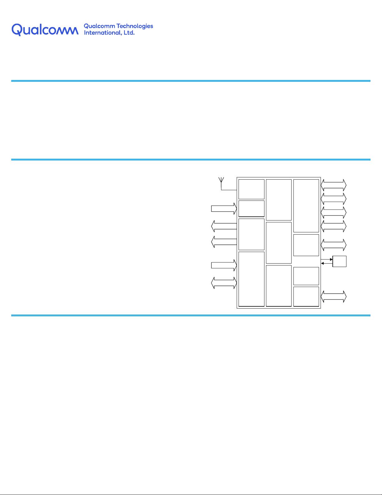
System architecture
XTAL
Ext Memory
Bluetooth
Radio
Digital
Audio
Interface
I/O
and
USB
Qualcomm
®
Kalimba™
DSP
Apps
Developer
Processor
Apps
Firmware
Processor
UART/USB
PIO
I²C/SPI
Stereo HQ
ADC
Stereo
Class-D or
Class-AB
Headphones
or
Line Out
LED Driver
with PWM
SMPS
LDOs
Li-Ion
Charger
Line In / Dual
Analog Mic In
OR
Headphones
Line Out
I²S/PCM
Battery
LED
DigMic
Confidential and Proprietary – Qualcomm Technologies International, Ltd.
NO PUBLIC DISCLOSURE PERMITTED: Please report postings of this document on public servers or websites to DocCtrlAgent@qualcomm.com.
Restricted Distribution: Not to be distributed to anyone who is not an employee of either Qualcomm T
echnologies International, Ltd. or its affiliated companies
without the express approval of Qualcomm Configuration Management.
Not to be used, copied, reproduced, or modified in whole or in part, nor its contents revealed in any manner to others without the express written permission of
Qualcomm Technologies International, Ltd.
All Qualcomm products mentioned herein are products of Qualcomm Technologies, Inc. and/or its subsidiaries. All Qualcomm products mentioned herein are
products of Qualcomm Technologies, Inc. and/or its subsidiaries.
Qualcomm and Qualcomm TrueWireless are trademarks of Qualcomm Incorporated, registered in the United States and other countries. Kalimba and Kymera are
trademarks of Qualcomm Technologies International, Ltd. cVc is a trademark of Qualcomm Technologies International, Ltd., registered in the United States and
other countries. Other product and brand names may be trademarks or registered trademarks of their respective owners.
This technical data may be subject to U.S. and international export, re-export, or transfer ("export") laws. Diversion contrary to U.S. and international law is strictly
prohibited.
Qualcomm Technologies International, Ltd. (formerly known as Cambridge Silicon Radio Limited) is a company registered in England and Wales with a registered
office at: Churchill House, Cambridge Business Park, Cowley Road, Cambridge, CB4 0WZ, United Kingdom.
Registered Number: 3665875 | VAT number: GB787433096
©
2018 Qualcomm Technologies, Inc. and/or its subsidiaries. All rights reserved.
QCC3024 VFBGA
Production Information
Data Sheet
80-CG232-1 Rev. AA
June 19, 2018


剩余80页未读,继续阅读

llc603
- 粉丝: 29
- 资源: 42
 我的内容管理
收起
我的内容管理
收起
- 我的资源
快来上传第一个资源
 我的收益 登录查看自己的收益
 我的积分
登录查看自己的积分
我的积分
登录查看自己的积分
 我的C币
登录后查看C币余额
我的C币
登录后查看C币余额
 我的收藏
我的收藏  我的下载
我的下载  下载帮助
下载帮助

会员权益专享


最新资源
- 2023年中国辣条食品行业创新及消费需求洞察报告.pptx
- 2023年半导体行业20强品牌.pptx
- 2023年全球电力行业评论.pptx
- 2023年全球网络安全现状-劳动力资源和网络运营的全球发展新态势.pptx
- 毕业设计-基于单片机的液体密度检测系统设计.doc
- 家用清扫机器人设计.doc
- 基于VB+数据库SQL的教师信息管理系统设计与实现 计算机专业设计范文模板参考资料.pdf
- 官塘驿林场林防火(资源监管)“空天地人”四位一体监测系统方案.doc
- 基于专利语义表征的技术预见方法及其应用.docx
- 浅谈电子商务的现状及发展趋势学习总结.doc
- 基于单片机的智能仓库温湿度控制系统 (2).pdf
- 基于SSM框架知识产权管理系统 (2).pdf
- 9年终工作总结新年计划PPT模板.pptx
- Hytera海能达CH04L01 说明书.pdf
- 数据中心运维操作标准及流程.pdf
- 报告模板 -成本分析与报告培训之三.pptx
资源上传下载、课程学习等过程中有任何疑问或建议,欢迎提出宝贵意见哦~我们会及时处理!
点击此处反馈


评论0