DAC0832:8位微处理器兼容双缓冲D/A转换器详解
DAC0830/DAC0832是一款先进的8位μP兼容型双缓冲数字模拟转换器,专为与8080、8048、8085、Z80等流行微处理器直接接口设计。这些器件采用CMOS/Si-Cr工艺,其中集成的R-2R电阻网络能够将参考电流进行细分,确保电路在不同温度下具有出色的线性度,最大满量程温度漂移仅为0.05%。低功耗设计通过使用CMOS电流开关和控制逻辑得以实现,同时输出泄露电流误差也得到了优化。
特别之处在于其双缓冲功能,允许在输出一个数字字节的同时,保持下一个数字字节稳定。这种特性使得多个DAC可以同时更新,提高了数据处理的效率和灵活性。DAC0830系列作为MICRO-DAC™家族的一部分,提供了多种输入模式,包括双缓冲、单缓冲和流通过数据输入,方便用户根据应用需求灵活选择。
除了上述特点,这些器件还具有易于与12位DAC1230系列替换或接插兼容的优势,这意味着它们可以在不改变现有系统布局的情况下提供更高精度的模拟输出。直接接口的设计减少了系统复杂性和所需的外围电路,简化了集成过程。
总体而言,DAC0830/DAC0832是一款高效、灵活且兼容性强的8位模拟信号生成器,适用于对数据传输速度、精度和电源效率有高要求的微处理器应用,如音频处理、工业控制系统和模拟信号合成等领域。设计者可以根据项目需求选择合适的接口模式,以实现最佳性能和成本效益。
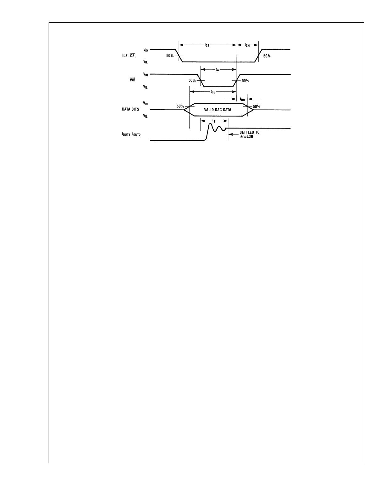
Switching Waveform
00560802
DAC0830/DAC0832
www.national.com 6
剩余27页未读,继续阅读
点击了解资源详情
105 浏览量
点击了解资源详情
496 浏览量
310 浏览量
点击了解资源详情
1527 浏览量

u010332932
- 粉丝: 0
- 资源: 3
 我的内容管理
展开
我的内容管理
展开


