没有合适的资源?快使用搜索试试~ 我知道了~
首页以太网PHY芯片STE100P手册
The STE100P, also referred to as STEPHY1, is a high performance Fast Ethernet physical layer interface for 10Base-T and 100Base-TX applications. It was designed with advanced CMOS technology to provide a Media Independent Interface (MII) for easy attachment to 10/100 Media Access Controllers (MAC) and a physical media interface for 100Base-TX of IEEE802.3u and 10Base-T of IEEE802.3. The STEPHY1 supports both half-duplex and fullduplex operation, at 10 and 100 Mbps operation. Its operating mode can be set using auto-negotiation, parallel detection or manual control. It also allows for the support of auto-negotiation functions for speed and duplex detection.
资源详情
资源评论
资源推荐

1/31
STE100P
February 2006
1 DESCRIPTION
The STE100P, also referred to as STEPHY1, is a
high performance Fast Ethernet physical layer in-
terface for 10Base-T and 100Base-TX applica-
tions.
It was designed with advanced CMOS technology
to provide a Media Independent Interface (MII) for
easy attachment to 10/100 Media Access Control-
lers (MAC) and a physical media interface for
100Base-TX of IEEE802.3u and 10Base-T of
IEEE802.3.
The STEPHY1 supports both half-duplex and full-
duplex operation, at 10 and 100 Mbps operation.
Its operating mode can be set using auto-negotia-
tion, parallel detection or manual control. It also al-
lows for the support of auto-negotiation functions
for speed and duplex detection.
2FEATURES
2.1 Industry standard
■ IEEE802.3u 100Base-TX and IEEE802.3
10Base-T compliant
■ Support for IEEE802.3x flow control
■ IEEE802.3u Auto-Negotiation support for
10Base-T and 100Base-TX
■ MII interface
■ Standard CSMA/CD or full duplex operation
supported
■ Industrial temperature compliant
10/100 FAST ETHERNET 3.3V TRANSCEIVER
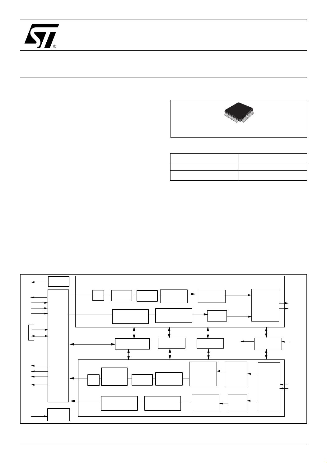
Figure 2. Block Diagram
NRZ To Manchester
Encoder
MII
Interface / Controller
10 TX
Filter
TRANSMITTER
10/100
Scrambler
Auto
Negotiation
4B/5B
NRZ To NRZI
Encoder
Link Pulse
Generator
Binary To MLT3
Encoder
RECEIVER
10/100
Parallel to
Serial
Descrambler
Code Align
4B/5B
NRZI To NRZ
Decoder
Serial to
Parallel
NRZ To Manchester
Encoder
Link Pulse
Detector
SMART
Squelch
10 TX Filter
Clock Recovery
Clock
Generation
System
Clock
Adaptive
Equalization
BaseLine
Wander
Binary To MLT3
Decoder
Clock Recovery
REGISTERS
HW Config
Power Down
LEDS
RX Channel
TX Channel
TXP
TXN
RXP
RXN
MDC
MDIO
RXD[3:0]
RX_ER
RX_DV
RX_CLK
TX_CLK
TXD[3:0]
TX_ER
TX_EN
LEDS
HW
configuration
pins
Serial Management
10Mb/s
100Mb/s
100Mb/s
10Mb/s
Loopback
Rev. 19
Fi
gure 1.
P
ac
k
age
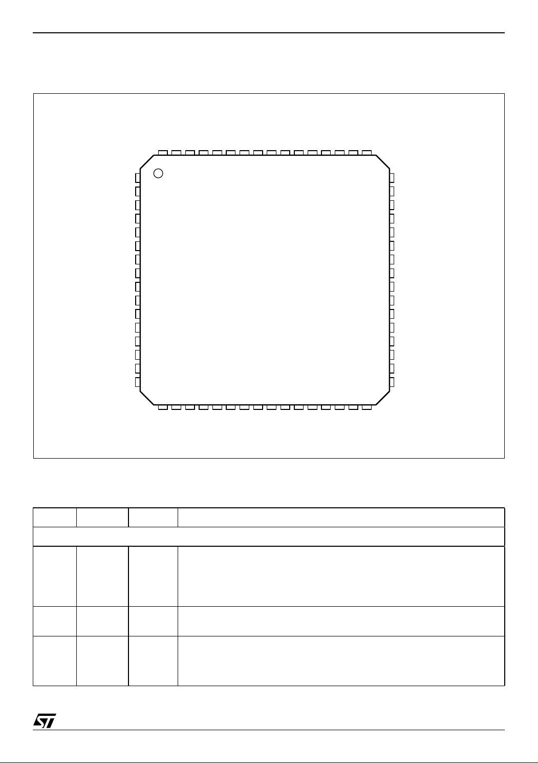
Table 1. Order Codes
(*) ECOPACK® (see
Section 9
)
Part Number Package
STE100P TQFP64
E-STE100P
(*)
TQFP64
TQFP64 (10x10x1.40mm)

STE100P
2/31
2.2 Physical Layer
■ Integrates the whole Physical layer functions of 100Base-TX and 10Base-T
■ Provides Full-duplex operation on both 100Mbps and 10Mbps modes
■ Provides Auto-negotiation(NWAY) function of full/half duplex operation for both 10 and 100 Mbps
■ Provides MLT-3 transceiver with DC restoration for Base-line wander compensation
■ Provides transmit wave-shaper, receive filters, and adaptive equalizer
■ Provides loop-back modes for diagnostic
■ Builds in Stream Cipher Scrambler/ De-scrambler and 4B/5B encoder/decoder
■ Supports external transmit transformer with turn ratio 1:1
■ Supports external receive transformer with turn ratio 1:1
2.3 LED Display
The LED display, consists of five LEDs having the following characteristics:
■ 10 Mbps Speed LED: 10Mbps(on) or 100Mbps(off)
■ 100 Mbps Speed LED: 100Mbps(on) or 10Mbps(off)
■ TX/RX Activity LED: Blinks at 10Hz when receiving, but not colliding
■ Link LED: On when a good link is detected, blinks when there is TX or RX activity
■ Full Duplex / Collision LED: On during Full Duplex operation. Blinks at 20Hz to indicate a collision
2.4 Miscellaneous
■ Standard 64-pin QFP package pinout
Figure 3. System Diagram of the STE100P Application
Boot ROM
25 MHz
Crystal
RJ-45
STE100P
STEPHY1
Serial
EEPROM
LEDs
PCI Interface
MAC
Device
Transformer

3/31
STE100P
3 PIN ASSIGNMENT DIAGRAM
Figure 4. Pin Connection
4 PIN DESCRIPTION
Table 2. Pin Description
Pin No. Name Type Description
MII Data Interface
52
58
57
56
55
txd4
txd3
txd2
txd1
txd0
I Transmit Data. The Media Access Controller (MAC) drives data to the STE100P
using these inputs.
txd4 is monitored only in Symbol (5B) Mode.
These signals must be synchronized to the tx_clk.
54 tx_en I Transmit Enable. The MAC asserts this signal when it drives valid data on the
txd inputs. This signal must be synchronized to the tx_clk.
53 tx_clk I/O Transmit Clock. Normally the STE100P drives tx_clk. Refer to the Clock
Requirements discussion in the Functional Description section.
25 MHz for 100 Mbps operation.
2.5 MHz for 10 Mbps operation.
1
2
3
5
6
4
7
8
9
10
27
11
28 29 30 31 32
59 58 57 56
54
55 53 52 51 50 49
43
42
41
39
38
40
48
47
46
44
45
fde
mf0
mf1
mf3
mf4
mf2
x2
gnda
vcca
gnda
nc
vcca
txn
gnda
gnde
pwrdwn
test
reset
rip
nc
nc
nc
col
txd3
txd2
txd1
tx_en
txd0
tx_clk
tx_er/txd4
rx_er/rxd4
gnde/i
rx_clk
rdx3
mdc
mdio
vcce/i
ledr10
gnde/i
rx_dv
rxd0
rxd1
rdx2
vcce/i
D99TL457B
22 23 24 25 26
60
crs
61
mdint
62
vcce/i
63
cfg1
64
cfg0
vcca
rxn
rxp
gnda
txp
17 18 19 20 21
37
36
34
33
35
ledtr
ledl
leds
test_se
ledc
12
13
14
15
16
vcca
iref
gnda
x1
vcca

STE100P
4/31
52 tx_er I Transmit Coding Error. The MAC asserts this input when an error has occurred
in the transmit data stream. When the STE100P is operating at 100 Mbps, the
STE100P responds by sending invalid code symbols on the line. In Symbol (5B)
Mode this pin functions as txd4.
51
43
44
46
47
rxd4
rxd3
rxd2
rxd1
rxd0
O Receive Data. The STE100P drives received data on these outputs, synchro-
nous to rx_clk.
rxd4 is driven only in Symbol (5B) Mode.
48 rx_dv O Receive Data Valid. The STE100P asserts This signal when it drives valid data
on rxd. This output is synchronous to rx_clk.
51 rx_er O Receive Error. The STE100P asserts this output when it receives invalid sym-
bols from the network. This signal is synchronous to rx_clk. In Symbol (5B) Mode
this pin functions as rxd4.
49 rx_clk O Receive Clock. This continuous clock provides reference for rxd, rx_dv, and
rx_er signals. Refer to the Clock Requirements discussion in the Functional
Description section.
25 MHz for 100 Mbps operation.
2.5 MHz for 10 Mbps operation.
59 col O Collision Detected. The STE100P asserts this output when detecting a collision.
This output remains High for the duration of the collision. This signal is asynchro-
nous and inactive during full-duplex operation.
60 crs O Carrier Sense. During half-duplex operation (PR0:8=0), the STE100P asserts
this output when either transmit or receive medium is non idle. During full duplex
operation (PR0:8=1), crs is asserted only when the receive medium is non-idle.
MII Control Interface
42 mdc I Management Data Clock. Clock for the mdio serial data channel. Maximum
frequency is 2.5 MHz.
41 mdio I/O Management Data Input/Output, Bi-directional serial data channel for PHY
communication.
61 mdint OD Management Data Interrupt. When any bit in PR18 = 1, an active High output
on this pin indicates status change in the corresponding bits in PR17.
Interrupt is cleared by reading Register PR17. Requires MDC edge to output.
Physical (Twisted Pair) Interface
12 x1 I 25 MHz reference clock input. When an external 25 MHz crystal is used, this pin
will be connected to one terminal of it. If an external 25 MHz clock source of
oscillator is used, then this pin will be the input pin of it.
11 x2 O 25 MHz reference clock output. When an external 25MHz crystal is used, this pin
will be connected to another terminal of if. If an external clock source is used,
then this pin should be left open.
21
23
txp
txn
O The differential Transmit outputs of 100Base-TX or 10Base-T, these pins directly
output to the transformer.
19
18
rxp
rxn
I The differential Receive inputs of 100Base-TX or 10Base-T, these pins directly
input from the transformer.
Table 2. Pin Description (continued)
Pin No. Name Type Description

5/31
STE100P
15 iref O Reference Resistor connecting pin for reference current, directly connect a 5KΩ ±
1% resistor to Vss.
38 ledr10 I/O LED display for 10Ms/s link status. This pin will be driven on continually when
10Mb/s network operating speed is detected.
The pull-up/pull-down status of this pin is latched into the PR20 bit 7 during
power up/reset.
37 ledtr LED display for Tx/Rx Activity status. This pin will be driven on at a 10 Hz blinking
frequency when either effective receiving or transmitting is detected.
The status of this pin is latched into the PR20 bit 6 during power up/reset.
36 ledl I/O LED display for Link Status. Blinks when there is TX or RX activity. This pin will be
driven on continually when a good Link test is detected.
The status of this pin is latched into the PR20 bit 5 during power up/reset.
35 ledc I/O LED display for Full Duplex or Collision status. This pin will be driven on
continually when a full duplex configuration is detected. This pin will be driven on
at a 20 Hz blinking frequency when a collision status is detected in the half duplex
configuration.
The status of this pin is latched into the PR20 bit 4 during power up/reset.
34 leds I/O LED display for 100Ms/s link status. This pin will be driven on continually when
100Mb/s network operating speed is detected.
The status of this pin is latched into the PR20 bit 3 during power up/reset.
64 cfg0 I Configuration Control 0.
When A/N is enabled, cfg0 determines operating mode advertisement
capabilities in combination with cfg1 when mf0/ PR0:12 =1. (See Table 2)
When A/N is disabled, cfg1 disables mlt3 and directly affects PR19:0
When cfg0 is Low, mlt3 encoder/decoder is enabled and PR19:1 =0.
When cfg0 is High, mlt3 encoder/decoder is bypassed and PR19:1 = 1.
63 cfg1 I Configuration Control 1.
When A/N is enabled, cfg1 determines operating mode advertisement
capabilities in combination with cfg1 when mf0/ PR0:12 =1. (See Table 2)
When A/N is disabled, CFG1 enables Loopback mode and directly affects PR0
bit 14.
When cfg1 is Low, Loopback mode is disabled and PR0:14 = 0.
When cfg1 is High, Loopback mode is enabled and PR0:14 = 1.
28 reset I Reset (Active-Low). This input must be held low for a minimum of 1 ms to reset
the STE100P. During Power-up, the STE100P will be reset regardless of the state
of this pin, and this reset will not be complete until after >1ms.
29 rip O Reset In Progress. This output is used to indicate when the device has
completed power-up/reset and the registers and functions can be accessed.
When rip is High, power-up/reset has been successful and the device can be
used normally
When rip is Low, device reset is not complete.
8, 30,31,
32
nc nc (No Connection)
26, 33 test,
test_se
Test pins. Should be tied to ground for normal operation
27 pwrdwn I Power Down. When High, forces STE100P into Power Down mode. This pin is
OR’ed with the Power Down bit (PR0:11). During the Power Down mode, txp/txn
outputs and all LED outputs are 3-stated, and the MII interface is isolated.
Table 2. Pin Description (continued)
Pin No. Name Type Description
剩余30页未读,继续阅读


zoogar
- 粉丝: 36
- 资源: 18
上传资源 快速赚钱
我的内容管理 收起
我的资源 快来上传第一个资源
我的收益
登录查看自己的收益我的积分 登录查看自己的积分
我的C币 登录后查看C币余额
我的收藏
我的下载
下载帮助

会员权益专享
安全验证
文档复制为VIP权益,开通VIP直接复制

评论0