

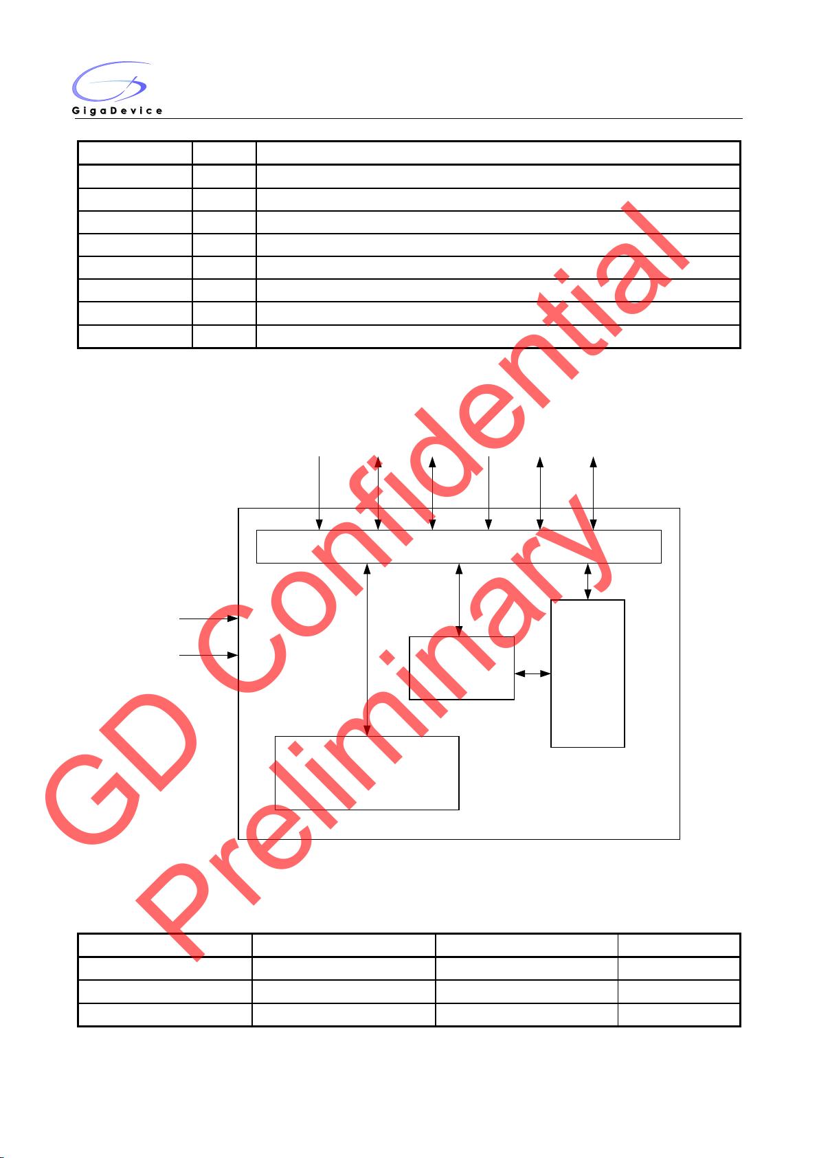
SPI(x1/x2/x4) NAND Flash GD5F1GQ4UAYIG
1
SPI (Serial Peripheral Interface) NAND Flash Memory
FEATURE
◆ 1G-bit Serial NAND Flash ◆ Program/Erase/Read Speed
-128M-byte -Page Program time: 400us typical
-2048 bytes page for read and program, spare 64bytes -Block Erase time: 3ms typical
-(128K + 4K)bytes per block for erase
-Page read time: 120us maximum(w/I ECC)
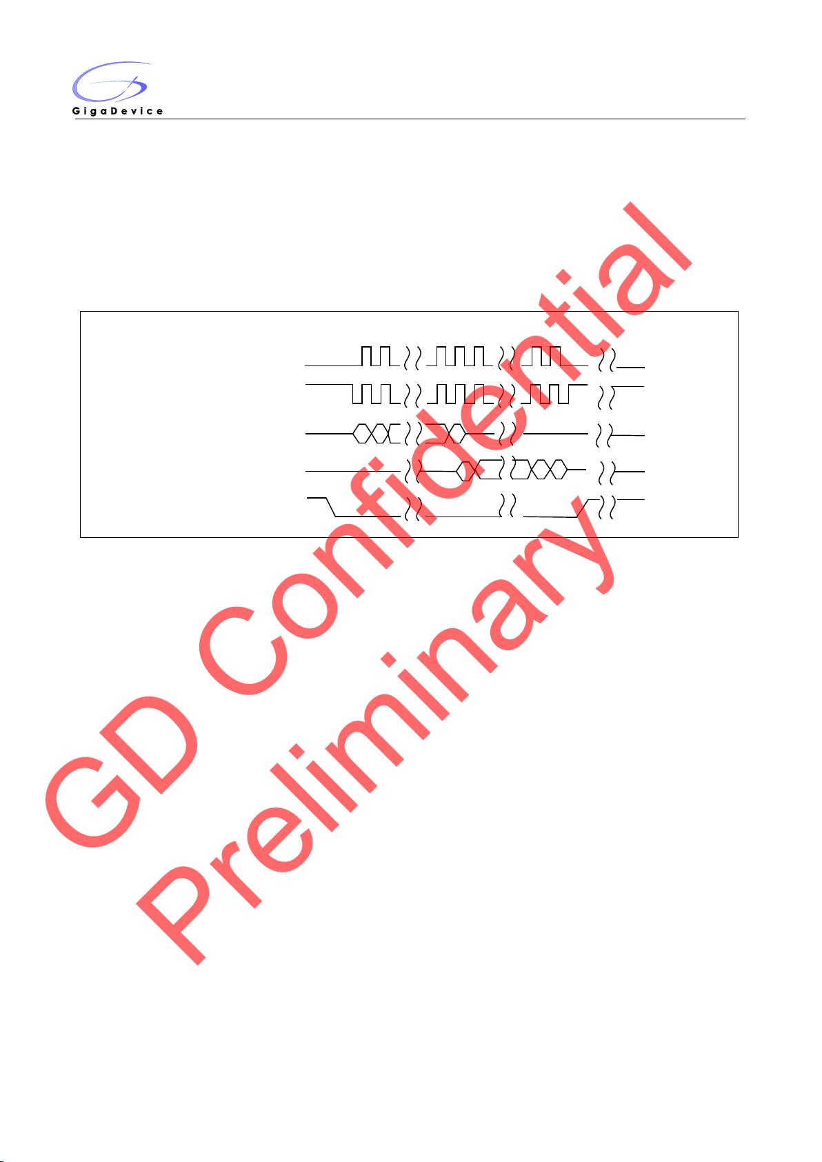
◆ Standard, Dual, Quad SPI ◆ Low Power Consumption
-Standard SPI: SCLK, CS#, SI, SO, WP#, HOLD# -40mA maximum active current
-Dual SPI: SCLK, CS#, SIO0, SIO1, WP#, HOLD# -70uA maximum standby current
-Quad SPI: SCLK, CS#, SIO0, SIO1, SIO2, SIO3
◆ High Speed Clock Frequency ◆ Enhanced access performance
-108MHz for fast read with 30PF load -2kbyte cache for fast random read
-Quad I/O Data transfer up to 480Mbits/s -Cache read and cache program
-2112/2048/64/16 wrap read option
◆ Software/Hardware Write Protection ◆ Advanced Feature for NAND
-Write protect all/portion of memory via software -Internal ECC option, per 512bytes
-Enable/Disable protection with WP# Pin -Internal data move by page with ECC
-Top or Bottom, Block selection combination -Promised golden block0
◆ Advanced security Features
-8K-Byte OTP Region
◆ Single Power Supply Voltage
-Full voltage range:2.7~3.6V
Note: please contact GigaDevice for details
GD Confidential
Preliminary

剩余31页未读,继续阅读

mirkerson
- 粉丝: 1399
- 资源: 5
 我的内容管理
收起
我的内容管理
收起
- 我的资源
快来上传第一个资源
 我的收益 登录查看自己的收益
 我的积分
登录查看自己的积分
我的积分
登录查看自己的积分
 我的C币
登录后查看C币余额
我的C币
登录后查看C币余额
 我的收藏
我的收藏  我的下载
我的下载  下载帮助
下载帮助

会员权益专享


最新资源
- 27页智慧街道信息化建设综合解决方案.pptx
- 计算机二级Ms-Office选择题汇总.doc
- 单链表的插入和删除实验报告 (2).docx
- 单链表的插入和删除实验报告.pdf
- 物联网智能终端项目设备管理方案.pdf
- 如何打造品牌的模式.doc
- 样式控制与页面布局.pdf
- 武汉理工Java实验报告(二).docx
- 2021线上新品消费趋势报告.pdf
- 第3章 Matlab中的矩阵及其运算.docx
- 基于Web的人力资源管理系统的必要性和可行性.doc
- 基于一阶倒立摆的matlab仿真实验.doc
- 速运公司物流管理模式研究教材
- 大数据与管理.pptx
- 单片机课程设计之步进电机.doc
- 大数据与数据挖掘.pptx
资源上传下载、课程学习等过程中有任何疑问或建议,欢迎提出宝贵意见哦~我们会及时处理!
点击此处反馈


评论2