
IMX117CQT
Contents
Description ......................................................................................................................................................................1
Features
..........................................................................................................................................................................1
Device Structure
..............................................................................................................................................................2
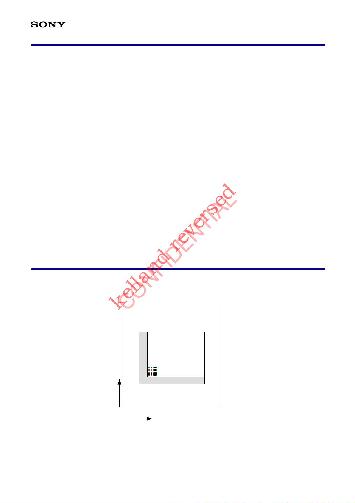
Optical Black Array and Readout Scan Direction
...............................................................................................................2
Absolute Maximum Ratings
..............................................................................................................................................3
Recommended Operating Conditions
...............................................................................................................................3
USE RESTRICTION NOTICE
..........................................................................................................................................4
Contents
..........................................................................................................................................................................5
Pin Configuration
.............................................................................................................................................................6
Pin Description
................................................................................................................................................................7
Electrical Characteristics
..................................................................................................................................................9
1. DC Characteristics
....................................................................................................................................................9
2. AC Characteristics
.................................................................................................................................................. 11
3. LVDS output
........................................................................................................................................................... 13
I/O Equivalent Circuit Diagram
....................................................................................................................................... 14
Spectral Sensitivity Characteristics
................................................................................................................................. 19
Image Sensor Characteristics
........................................................................................................................................ 20
1. Zone Definition of Video Signal Shading
.................................................................................................................. 20
Image Sensor Characteristics Measurement Method
...................................................................................................... 21
1. Measurement Conditions
........................................................................................................................................ 21
2. Color Coding of this Image Sensor and Readout
..................................................................................................... 21
3. Definition of Standard Imaging Conditions
............................................................................................................... 21
Setting Registers by Serial Communication
.................................................................................................................... 23
Register Map
................................................................................................................................................................. 24
1. Register Value Reflection Timing to Output Data
...................................................................................................... 28
2. Description of Register
........................................................................................................................................... 29
3. Register Setting for Each Readout Drive Mode
........................................................................................................ 39
3-1. When Using Type 1/2.3 Approx. 12.40 M Pixels (4:3)
......................................................................................... 39
3-2. When Using Type 1/2.5 Approx. 9.03 M Pixels (Approx. 17:9)
............................................................................ 41
3-3. When Using Type 1/4.4 Approx. 3.09 M Pixels (16:9)
......................................................................................... 43
1. Readout Drive Modes
............................................................................................................................................. 45
1-1. When Using Type 1/2.3 Approx. 12.40 M Pixels (4:3)
......................................................................................... 45
1-2. When Using Type 1/2.5 Approx. 9.03 M Pixels (Approx. 17:9)
............................................................................ 46
1-3. When Using Type 1/4.4 Approx. 3.09 M Pixels (16:9)
......................................................................................... 46
1-4. Relationship between Arithmetic Processing and the Number of Output Bits in Each Readout Drive Mode
.......... 47
2. Sync Signals and Data Output Timing
..................................................................................................................... 50
3. Output Range of LVDS Output Data
........................................................................................................................ 52
4. Detailed Specification of Each Mode
....................................................................................................................... 53
4-1. When Using Type 1/2.3 Approx. 12.40 M Pixels (4:3)
......................................................................................... 53
(1) Horizontal/Vertical Operation Period in Each Readout Drive Mode
................................................................... 53
(2) NTSC/PAL Compatible Drive
.......................................................................................................................... 54
(3) Image Data Output Format
............................................................................................................................. 55
4-2. When Using Type 1/2.5 Approx. 9.03 M Pixels (Approx. 17:9)
............................................................................ 67
(1) Horizontal/Vertical Operation Period in Each Readout Drive Mode
................................................................... 67
(2) NTSC/PAL Compatible Drive
.......................................................................................................................... 68
(3) Image Data Output Format
............................................................................................................................. 69
4-3. When Using Type 1/4.4 Approx. 3.09 M Pixels (16:9)
......................................................................................... 78
(1) Horizontal/Vertical Operation Period in Each Readout Drive Mode
................................................................... 78
(2) NTSC/PAL Compatible Drive
.......................................................................................................................... 78
(3) Image Data Output Format
............................................................................................................................. 79
Integration Time in Each Readout Drive Mode and Mode Changes
.................................................................................. 80
1. Integration Time in Each Readout Drive Mode
......................................................................................................... 80
2. Operation when Changing the Readout Drive Mode
................................................................................................ 82
3. Recommended Global Reset Shutter Operation Sequence
...................................................................................... 83
4. Interrupt Mode Change
........................................................................................................................................... 85
Power-on/off Sequence
.................................................................................................................................................. 86
1. Power-on Sequence
............................................................................................................................................... 86
2. Power-off Sequence
............................................................................................................................................... 87
Standby Cancel Sequence
............................................................................................................................................. 88
Peripheral Circuit Diagram
............................................................................................................................................. 89
Notes On Handling
........................................................................................................................................................ 90
Package Outline
............................................................................................................................................................ 92
kelland reversed


 我的内容管理
收起
我的内容管理
收起
 我的收益 登录查看自己的收益
 我的积分
登录查看自己的积分
我的积分
登录查看自己的积分
 我的C币
登录后查看C币余额
我的C币
登录后查看C币余额
 我的收藏
我的收藏  我的下载
我的下载  下载帮助
下载帮助 


评论0