没有合适的资源?快使用搜索试试~ 我知道了~
首页EFM8SB1小蜜蜂单片机手册Silicon-Labs
资源详情
资源评论
资源推荐
EFM8 Sleepy Bee Family
EFM8SB1 Data Sheet
The EFM8SB1, part of the Sleepy Bee family of MCUs, is the
world’s most energy friendly 8-bit microcontrollers with a compre-
hensive feature set in small packages.
These devices offer lowest power consumption by combining innovative low energy tech-
niques and short wakeup times from energy saving modes into small packages, making
them well-suited for any battery operated applications. With an efficient 8051 core, 14
high-quality capacitive sense channels, and precision analog, the EFM8SB1 family is al-
so optimal for embedded applications.
EFM8SB1 applications include the following:
ENERGY FRIENDLY FEATURES
• Lowest MCU sleep current with supply
brownout (50 nA)
• Lowest MCU active current (150 μA / MHz
at 24.5 MHz)
• Lowest MCU wake on touch average
current (< 1 μA)
• Lowest sleep current using internal RTC
and supply brownout (< 300 nA)
• Ultra-fast wake up for digital and analog
peripherals (< 2 μs)
• Integrated LDO to maintain ultra-low active
current at all voltages
• Touch pads / key pads
• Wearables
• Instrumentation panels
• Battery-operated consumer electronics
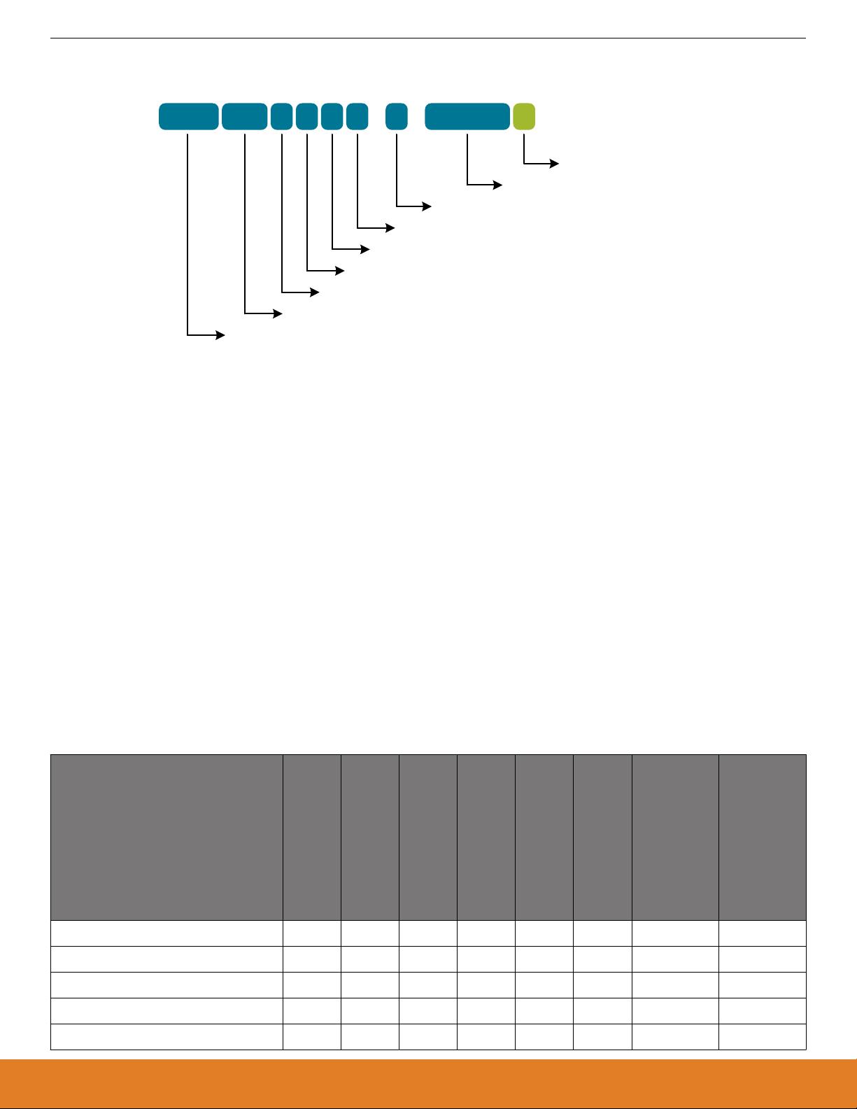
SecurityAnalog Interfaces
Comparator 0
Internal Voltage
Reference
Internal Current
Reference
ADC
Capacitive Sense
I/O Ports
Core / Memory Clock Management
CIP-51 8051 Core
(25 MHz)
Energy Management
Internal LDO
Regulator
Brown-Out Detector
Power-On Reset
8-bit SFR bus
Serial Interfaces Timers and Triggers
SPI
Pin Reset
Timers
0/1/2/3
PCA/PWM
Watchdog
Timer
16-bit CRC
Flash Program
Memory
(up to 8 KB)
RAM Memory
(up to 512 bytes)
Debug Interface
with C2
Lowest power mode with peripheral operational:
IdleNormal Suspend Sleep
High Frequency
24.5 MHz RC
Oscillator
Pin Wakeup
External
Interrupts
General
Purpose I/O
I
2
C / SMBus
UART
Low Frequency
RC Oscillator
External 32 kHz RTC Oscillator
Low Power 20 MHz
RC Oscillator
External
Oscillator
Real Time
Clock
silabs.com | Smart. Connected. Energy-friendly. Rev. 1.1
1. Feature List
The EFM8SB1 highlighted features are listed below.
• Core:
• Pipelined CIP-51 Core
• Fully compatible with standard 8051 instruction set
• 70% of instructions execute in 1-2 clock cycles
• 25 MHz maximum operating frequency
• Memory:
• Up to 8 kB flash memory, in-system re-programmable
from firmware.
• Up to 512 bytes RAM (including 256 bytes standard 8051
RAM and 256 bytes on-chip XRAM)
• Power:
• Internal LDO regulator for CPU core voltage
• Power-on reset circuit and brownout detectors
• I/O: Up to 17 total multifunction I/O pins:
• Flexible peripheral crossbar for peripheral routing
• 5 mA source, 12.5 mA sink allows direct drive of LEDs
• Clock Sources:
• Internal 20 MHz low power oscillator with ±10% accuracy
• Internal 24.5 MHz precision oscillator with ±2% accuracy
• Internal 16.4 kHz low-frequency oscillator or RTC 32 kHz
crystal
• External crystal, RC, C, and CMOS clock options
• Timers/Counters and PWM:
• 32-bit Real Time Clock (RTC)
• 3-channel Programmable Counter Array (PCA) supporting
PWM, capture/compare, and frequency output modes with
watchdog timer function
• 4 x 16-bit general-purpose timers
• Communications and Digital Peripherals:
• UART
• SPI™ Master / Slave
• SMBus™ / I2C™ Master / Slave
• 16-bit CRC unit, supporting automatic CRC of flash at 256-
byte boundaries
• Analog:
• Capacitive Sense (CS0)
• Programmable current reference (IREF0)
• 12-Bit Analog-to-Digital Converter (ADC0)
• 1 x Low-current analog comparator
• On-Chip, Non-Intrusive Debugging
• Full memory and register inspection
• Four hardware breakpoints, single-stepping
• Pre-loaded UART bootloader
• Temperature range -40 to 85 ºC
• Single power supply 1.8 to 3.6 V
• QSOP24, QFN24, and QFN20 packages
With on-chip power-on reset, voltage supply monitor, watchdog timer, and clock oscillator, the EFM8SB1 devices are truly standalone
system-on-a-chip solutions. The flash memory is reprogrammable in-circuit, providing non-volatile data storage and allowing field up-
grades of the firmware. The on-chip debugging interface (C2) allows non-intrusive (uses no on-chip resources), full speed, in-circuit
debugging using the production MCU installed in the final application. This debug logic supports inspection and modification of memory
and registers, setting breakpoints, single stepping, and run and halt commands. All analog and digital peripherals are fully functional
while debugging. Each device is specified for 1.8 to 3.6 V operation and is available in 20-pin QFN, 24-pin QFN, or 24-pin QSOP pack-
ages. All package options are lead-free and RoHS compliant.
EFM8SB1 Data Sheet
Feature List
silabs.com | Smart. Connected. Energy-friendly. Rev. 1.1 | 1
2. Ordering Information
EFM8
SB1
–0 F 8 G A – QSOP24 R
Tape and Reel (Optional)
Package Type
Revision
Temperature Grade G (-40 to +85)
Flash Memory Size – 8 KB
Memory Type (Flash)
Family Feature Set
Sleepy Bee 1 Family
Silicon Labs EFM8 Product Line
Figure 2.1. EFM8SB1 Part Numbering
All EFM8SB1 family members have the following features:
• CIP-51 Core running up to 25 MHz
• Three Internal Oscillators (24.5 MHz, 20 MHz, and 16 kHz)
• SMBus / I2C
• SPI
• UART
• 3-Channel Programmable Counter Array (PWM, Clock Generation, Capture/Compare)
• 4 16-bit Timers
• Analog Comparator
• 6-bit current sourc reference
• 12-bit Analog-to-Digital Converter with integrated multiplexer, voltage reference, and temperature sensor
• 16-bit CRC Unit
• Pre-loaded UART bootloader
In addition to these features, each part number in the EFM8SB1 family has a set of features that vary across the product line. The
product selection guide shows the features available on each family member.
Table 2.1. Product Selection Guide
Ordering Part Number
Flash Memory (kB)
RAM (Bytes)
Digital Port I/Os (Total)
ADC0 Channels
Capacitive Touch Inputs
Pb-free (RoHS Compliant)
Temperature Range
Package
EFM8SB10F8G-A-QSOP24 8 512 17 10 14 Yes -40 to +85 C QSOP24
EFM8SB10F8G-A-QFN24 8 512 17 10 14 Yes -40 to +85 C QFN24
EFM8SB10F8G-A-QFN20 8 512 16 9 13 Yes -40 to +85 C QFN20
EFM8SB10F4G-A-QFN20 4 512 16 9 13 Yes -40 to +85 C QFN20
EFM8SB10F2G-A-QFN20 2 256 16 9 13 Yes -40 to +85 C QFN20
EFM8SB1 Data Sheet
Ordering Information
silabs.com | Smart. Connected. Energy-friendly. Rev. 1.1 | 2
3. System Overview
3.1 Introduction
Digital Peripherals
Analog Peripherals
AMUX
UART
Timers 0,
1, 2, 3
PCA/WDT
Priority
Crossbar
Decoder
Crossbar Control
Port I/O Configuration
CIP-51 8051 Controller
Core
8/4/2 KB ISP Flash
Program Memory
256 Byte SRAM
SFR
Bus
256 Byte XRAM
14-Channel
Capacitance
To Digital
Converter
SPI
Comparator
VDD
XTAL1
SYSCLK
System Clock
Configuration
External
Oscillator
Circuit
Precision
24.5 MHz
Oscillator
Debug /
Programming
Hardware
Power On
Reset/PMU
Reset
C2D
C2CK/RSTb
Wake
12-bit
ADC
Temp
Sensor
External
VREF
Internal
VREF
VDD
XTAL2
Low Power
20 MHz
Oscillator
6-bit
IREF
VREF
GND
IREF0
RTC
Oscillator
XTAL3
XTAL4
GND
VREG
Digital
Power
+
-
Port 0
Drivers
Port 1
Drivers
P0.n
Port 2
Driver
P2.n
P1.n
CRC
SMBus
Figure 3.1. Detailed EFM8SB1 Block Diagram
EFM8SB1 Data Sheet
System Overview
silabs.com | Smart. Connected. Energy-friendly. Rev. 1.1 | 3
3.2 Power
All internal circuitry draws power from the VDD supply pin. External I/O pins are powered from the VIO supply voltage (or VDD on devi-
ces without a separate VIO connection), while most of the internal circuitry is supplied by an on-chip LDO regulator. Control over the
device power can be achieved by enabling/disabling individual peripherals as needed. Each analog peripheral can be disabled when
not in use and placed in low power mode. Digital peripherals, such as timers and serial buses, have their clocks gated off and draw little
power when they are not in use.
Table 3.1. Power Modes
Power Mode Details Mode Entry Wake-Up Sources
Normal Core and all peripherals clocked and fully operational — —
Idle • Core halted
• All peripherals clocked and fully operational
• Code resumes execution on wake event
Set IDLE bit in PCON0 Any interrupt
Suspend • Core and digital peripherals halted
• Internal oscillators disabled
• Code resumes execution on wake event
1. Switch SYSCLK to
HFOSC0 or LPOSC0
2. Set SUSPEND bit in
PMU0CF
• RTC0 Alarm Event
• RTC0 Fail Event
• CS0 Interrupt
• Port Match Event
• Comparator 0 Rising
Edge
Sleep • Most internal power nets shut down
• Select circuits remain powered
• Pins retain state
• All RAM and SFRs retain state
• Code resumes execution on wake event
1. Disable unused ana-
log peripherals
2. Set SLEEP bit in
PMU0CF
• RTC0 Alarm Event
• RTC0 Fail Event
• Port Match Event
• Comparator 0 Rising
Edge
3.3 I/O
Digital and analog resources are externally available on the device’s multi-purpose I/O pins. Port pins P0.0-P1.7 can be defined as gen-
eral-purpose I/O (GPIO), assigned to one of the internal digital resources through the crossbar or dedicated channels, or assigned to an
analog function. Port pin P2.7 can be used as GPIO. Additionally, the C2 Interface Data signal (C2D) is shared with P2.7.
• Up to 17 multi-functions I/O pins, supporting digital and analog functions.
• Flexible priority crossbar decoder for digital peripheral assignment.
• Two drive strength settings for each pin.
• Two direct-pin interrupt sources with dedicated interrupt vectors (INT0 and INT1).
• Up to 16 direct-pin interrupt sources with shared interrupt vector (Port Match).
3.4 Clocking
The CPU core and peripheral subsystem may be clocked by both internal and external oscillator resources. By default, the system
clock comes up running from the 20 MHz low power oscillator divided by 8.
• Provides clock to core and peripherals.
• 20 MHz low power oscillator (LPOSC0), accurate to ±10% over supply and temperature corners.
• 24.5 MHz internal oscillator (HFOSC0), accurate to ±2% over supply and temperature corners.
• 16.4 kHz low-frequency oscillator (LFOSC0) or external RTC 32 kHz crystal.
• External RC, C, CMOS, and high-frequency crystal clock options (EXTCLK).
• Clock divider with eight settings for flexible clock scaling: Divide the selected clock source by 1, 2, 4, 8, 16, 32, 64, or 128.
EFM8SB1 Data Sheet
System Overview
silabs.com | Smart. Connected. Energy-friendly. Rev. 1.1 | 4
剩余46页未读,继续阅读
听风观雨处变不惊
- 粉丝: 4
- 资源: 24
上传资源 快速赚钱
- 我的内容管理 收起
- 我的资源 快来上传第一个资源
- 我的收益 登录查看自己的收益
- 我的积分 登录查看自己的积分
- 我的C币 登录后查看C币余额
- 我的收藏
- 我的下载
- 下载帮助
会员权益专享
最新资源
- RTL8188FU-Linux-v5.7.4.2-36687.20200602.tar(20765).gz
- c++校园超市商品信息管理系统课程设计说明书(含源代码) (2).pdf
- 建筑供配电系统相关课件.pptx
- 企业管理规章制度及管理模式.doc
- vb打开摄像头.doc
- 云计算-可信计算中认证协议改进方案.pdf
- [详细完整版]单片机编程4.ppt
- c语言常用算法.pdf
- c++经典程序代码大全.pdf
- 单片机数字时钟资料.doc
- 11项目管理前沿1.0.pptx
- 基于ssm的“魅力”繁峙宣传网站的设计与实现论文.doc
- 智慧交通综合解决方案.pptx
- 建筑防潮设计-PowerPointPresentati.pptx
- SPC统计过程控制程序.pptx
- SPC统计方法基础知识.pptx
资源上传下载、课程学习等过程中有任何疑问或建议,欢迎提出宝贵意见哦~我们会及时处理!
点击此处反馈
安全验证
文档复制为VIP权益,开通VIP直接复制
信息提交成功
评论1