没有合适的资源?快使用搜索试试~ 我知道了~
首页mpc5121e datasheet
资源详情
资源评论
资源推荐
Freescale Semiconductor
Data Sheet: Advance Information
Document Number: MPC5121E
Rev. 1, 10/2008
© Freescale Semiconductor, Inc., 2008. All rights reserved.
This document contains information on a product under development. Freescale reserves the
right to change or discontinue this product without notice.
MPC5121E/MPC5123
TEPBGA
27 mm x 27 mm
The MPC5121e/MPC5123 integrates a high performance
e300 CPU core based on the Power Architecture Technology
with a rich set of peripheral functions focused on
communications and systems integration.
Major features of the MPC5121e/MPC5123 are:
• e300 Power Architecture processor core (enhanced version
of the MPC603e core), operates up to 400 MHz
• Power modes include doze, nap, sleep, deep sleep, and
hibernate
• AXE – fully programmable, 200 MHz 32-bit RISC core for
real-time acceleration tasks, such as audio.
• MBX Lite – 2D/3D graphics engine with PowerVR vector
processing (only in MPC5121e, not in MPC5123)
• DIU – Display interface unit
• DDR1, DDR2, and low-power mobile DDR (LPDDR)
SDRAM memory controller
• USB 2.0 OTG controller with integrated physical layer
(PHY)
• DMA subsystem
• EMB – Flexible multi-function external memory bus
interface
• NFC – NAND flash controller
• 10/100Base Ethernet
• PCI interface, version 2.3
• PATA – Parallel ATA integrated development environment
(IDE) controller
• SATA – Serial ATA controller with integrated physical
layer (PHY)
• SDHC – MMC/SD/SDIO card host controller
• PSC – Programmable serial controller
• S/PDIF – Serial audio interface
• CAN – Controller area network
• BDLC – J1850 interface
• VIU – Video Input, ITU-656 complient
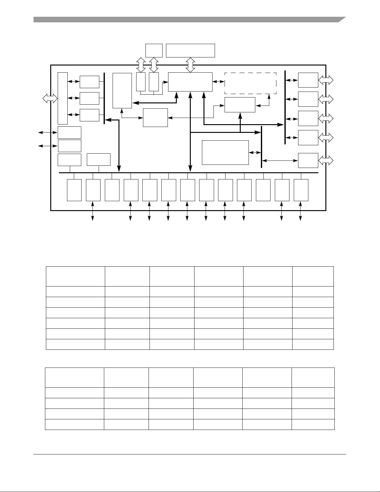
Figure 1 shows a simplified MPC5121e/MPC5123 block
diagram.
MPC5121E/MPC5123
Data Sheet
Preliminary
MPC5121E/MPC5123 Data Sheet, Rev. 1
Freescale Semiconductor2
Table of Contents
1 Ordering Information. . . . . . . . . . . . . . . . . . . . . . . . . . . . . . . . .3
2 Pin Assignments . . . . . . . . . . . . . . . . . . . . . . . . . . . . . . . . . . . .4
2.1 Pinout Listings. . . . . . . . . . . . . . . . . . . . . . . . . . . . . . . . .4
3 Electrical and Thermal Characteristics . . . . . . . . . . . . . . . . . .16
3.1 DC Electrical Characteristics . . . . . . . . . . . . . . . . . . . .16
3.1.1 Absolute Maximum Ratings . . . . . . . . . . . . . . . .16
3.1.2 Recommended Operating Conditions . . . . . . . .17
3.1.3 DC Electrical Specifications. . . . . . . . . . . . . . . .18
3.1.4 Electrostatic Discharge . . . . . . . . . . . . . . . . . . .20
3.1.5 Power Dissipation . . . . . . . . . . . . . . . . . . . . . . .22
3.1.6 Thermal Characteristics. . . . . . . . . . . . . . . . . . .23
3.2 Oscillator and PLL Electrical Characteristics . . . . . . . .24
3.2.1 System Oscillator Electrical Characteristics . . .25
3.2.2 RTC Oscillator Electrical Characteristics . . . . . .25
3.2.3 System PLL Electrical Characteristics. . . . . . . .25
3.2.4 e300 Core PLL Electrical Characteristics . . . . .26
3.3 AC Electrical Characteristics. . . . . . . . . . . . . . . . . . . . .27
3.3.1 Overview . . . . . . . . . . . . . . . . . . . . . . . . . . . . . .27
3.3.2 AC Operating Frequency Data. . . . . . . . . . . . . .27
3.3.3 Resets . . . . . . . . . . . . . . . . . . . . . . . . . . . . . . . .28
3.3.4 External Interrupts . . . . . . . . . . . . . . . . . . . . . . .31
3.3.5 SDRAM (DDR) . . . . . . . . . . . . . . . . . . . . . . . . .31
3.3.6 PCI. . . . . . . . . . . . . . . . . . . . . . . . . . . . . . . . . . .34
3.3.7 LPC . . . . . . . . . . . . . . . . . . . . . . . . . . . . . . . . . .35
3.3.8 NFC . . . . . . . . . . . . . . . . . . . . . . . . . . . . . . . . . .42
3.3.9 PATA. . . . . . . . . . . . . . . . . . . . . . . . . . . . . . . . . .44
3.3.10 SATA PHY . . . . . . . . . . . . . . . . . . . . . . . . . . . . .56
3.3.11 FEC . . . . . . . . . . . . . . . . . . . . . . . . . . . . . . . . . .56
3.3.12 USB ULPI. . . . . . . . . . . . . . . . . . . . . . . . . . . . . 58
3.3.13 On-Chip USB PHY . . . . . . . . . . . . . . . . . . . . . . 59
3.3.14 SDHC . . . . . . . . . . . . . . . . . . . . . . . . . . . . . . . . 59
3.3.15 DIU . . . . . . . . . . . . . . . . . . . . . . . . . . . . . . . . . . 61
3.3.16 SPDIF. . . . . . . . . . . . . . . . . . . . . . . . . . . . . . . . 64
3.3.17 CAN . . . . . . . . . . . . . . . . . . . . . . . . . . . . . . . . . 64
3.3.18 I
2
C . . . . . . . . . . . . . . . . . . . . . . . . . . . . . . . . . . 64
3.3.19 J1850 . . . . . . . . . . . . . . . . . . . . . . . . . . . . . . . . 65
3.3.20 PSC . . . . . . . . . . . . . . . . . . . . . . . . . . . . . . . . . 65
3.3.21 GPIOs and Timers . . . . . . . . . . . . . . . . . . . . . . 72
3.3.22 Fusebox . . . . . . . . . . . . . . . . . . . . . . . . . . . . . . 72
3.3.23 IEEE 1149.1 (JTAG). . . . . . . . . . . . . . . . . . . . . 73
3.3.24 VIU . . . . . . . . . . . . . . . . . . . . . . . . . . . . . . . . . . 75
4 System Design Information . . . . . . . . . . . . . . . . . . . . . . . . . . 75
4.1 Power Up/Down Sequencing . . . . . . . . . . . . . . . . . . . . 75
4.2 System and CPU Core AVDD Power Supply Filtering. 75
4.3 Connection Recommendations . . . . . . . . . . . . . . . . . . 76
4.4 Pull-Up/Pull-Down Resistor Requirements . . . . . . . . . 77
4.4.1 Pull-Down Resistor Requirements for TEST pin77
4.4.2 Pull-Up Requirements for the PCI Control Lines77
4.5 JTAG . . . . . . . . . . . . . . . . . . . . . . . . . . . . . . . . . . . . . . 77
4.5.1 TRST . . . . . . . . . . . . . . . . . . . . . . . . . . . . . . . . 77
4.5.2 e300 COP/BDM Interface . . . . . . . . . . . . . . . . 78
5 Package Information . . . . . . . . . . . . . . . . . . . . . . . . . . . . . . . 81
5.1 Package Parameters . . . . . . . . . . . . . . . . . . . . . . . . . . 82
5.2 Mechanical Dimensions. . . . . . . . . . . . . . . . . . . . . . . . 82
6 Product Documentation. . . . . . . . . . . . . . . . . . . . . . . . . . . . . 85
Preliminary
Ordering Information
MPC5121E/MPC5123 Data Sheet, Rev. 1
Freescale Semiconductor 3
Figure 1. Simplified MPC5121e/MPC5123 Block Diagram
1 Ordering Information
Table 1. MPC5121e Orderable Part Numbers
Freescale Part
Number
Speed (MHz)
Temperature
(ambient)
Qualification Package Availability
MPC5121VY400B 400 0
o
C to 70
o
C Consumer RoHS and Pb-free Tray
MPC5121VY400BR 400 0
o
C to 70
o
C Consumer RoHS and Pb-free Tape and Reel
MPC5121YVY400B 400 -40
o
C to 85
o
C Industrial RoHS and Pb-free Tray
MPC5121YVY400BR 400 -40
o
C to 85
o
C Industrial RoHS and Pb-free Tape and Reel
SPC5121YVY400B 400 -40
o
C to 85
o
C Automotive - AEC RoHS and Pb-free Tray
SPC5121YVY400BR 400 -40
o
C to 85
o
C Automotive - AEC RoHS and Pb-free Tape and Reel
Table 2. MPC5123 Orderable Part Numbers
Freescale Part
Number
Speed (MHz)
Temperature
(ambient)
Qualification Package Availability
MPC5123VY300B 300 0
o
C to 70
o
C Consumer RoHS and Pb-free Tray
MPC5123VY300BR 300 0
o
C to 70
o
C Consumer RoHS and Pb-free Tape and Reel
MPC5123YVY300B 300 -40
o
C to 85
o
C Industrial RoHS and Pb-free Tray
MPC5123YVY300BR 300 -40
o
C to 85
o
C Industrial RoHS and Pb-free Tape and Reel
PMC
IPIC
WDT
GPT
GPIO
I
2
C 3
CAN 4
J1850
SDHC
SPDIF
CFM
PSC 12
RTC
83 MHz (max) IP Bus
Display DDR1/2 Memory
Functionally
Multiplexed I/O
LPC
NFC
PATA
EMB
83 MHz IP Bus
AXE
Engine
8 KB
DIU
Multi-Port
Memory Controller
MBX Lite
Graphics Engine with
Vector Processing
FEC
USB2
+ PHY
USB2
ULPI
SATA
+ PHY
PCI
200 MHz AHB (32-Bit)
Te mp F use
128 KB
SRAM
DMA
64-Channel
e300
PowerPC™
32-KB I-/32-KB D-
Cache
200 MHz CSB
Bus (64-Bit)
RESET/
JTAG/COP
CLOCK
I-Cache
VIU
not available in MPC5123
Preliminary
MPC5121E/MPC5123 Data Sheet, Rev. 1
Pin Assignments
Freescale Semiconductor4
2 Pin Assignments
This section details pin assignments.
2.1 Pinout Listings
Table 3 provides the pin-out listing for the MPC5121e/MPC5123.
SPC5123YVY300B 300 -40
o
C to 85
o
C Automotive - AEC RoHS and Pb-free Tray
SPC5123YVY300BR 300 -40
o
C to 85
o
C Automotive - AEC RoHS and Pb-free Tape and Reel
MPC5123VY400B 400 0
o
C to 70
o
C Consumer RoHS and Pb-free Tray
MPC5123VY400BR 400 0
o
C to 70
o
C Consumer RoHS and Pb-free Tape and Reel
MPC5123YVY400B 400 -40
o
C to 85
o
C Industrial RoHS and Pb-free Tray
MPC5123YVY400BR 400 -40
o
C to 85
o
C Industrial RoHS and Pb-free Tape and Reel
SPC5123YVY400B 400 -40
o
C to 85
o
C Automotive - AEC RoHS and Pb-free Tray
SPC5123YVY400BR 400 -40
o
C to 85
o
C Automotive - AEC RoHS and Pb-free Tape and Reel
Table 3. MPC5121e/MPC5123 TE-PBGA Pinout Listing (Sheet 1 of 12)
Signal Package Pin Number Pad Type Power Supply Notes
DDR Memory Interface (67 Total)
MDQ0 AF5 DDR VDD_MEM_IO —
MDQ1 AB6 DDR VDD_MEM_IO —
MDQ2 AE4 DDR VDD_MEM_IO —
MDQ3 AF6 DDR VDD_MEM_IO —
MDQ4 AF7 DDR VDD_MEM_IO —
MDQ5 AB8 DDR VDD_MEM_IO —
MDQ6 AD6 DDR VDD_MEM_IO —
MDQ7 AE6 DDR VDD_MEM_IO —
MDQ8 AC7 DDR VDD_MEM_IO —
MDQ9 AF8 DDR VDD_MEM_IO —
MDQ10 AB9 DDR VDD_MEM_IO —
MDQ11 AD7 DDR VDD_MEM_IO —
MDQ12 AE9 DDR VDD_MEM_IO —
MDQ13 AF10 DDR VDD_MEM_IO —
MDQ14 AC9 DDR VDD_MEM_IO —
MDQ15 AF11 DDR VDD_MEM_IO —
Table 2. MPC5123 Orderable Part Numbers (continued)
Freescale Part
Number
Speed (MHz)
Temperature
(ambient)
Qualification Package Availability
Preliminary
Pin Assignments
MPC5121E/MPC5123 Data Sheet, Rev. 1
Freescale Semiconductor 5
MDQ16 AD10 DDR VDD_MEM_IO —
MDQ17 AF12 DDR VDD_MEM_IO —
MDQ18 AD11 DDR VDD_MEM_IO —
MDQ19 AB12 DDR VDD_MEM_IO —
MDQ20 AD12 DDR VDD_MEM_IO —
MDQ21 AB13 DDR VDD_MEM_IO —
MDQ22 AF14 DDR VDD_MEM_IO —
MDQ23 AD13 DDR VDD_MEM_IO —
MDQ24 AE13 DDR VDD_MEM_IO —
MDQ25 AC13 DDR VDD_MEM_IO —
MDQ26 AF15 DDR VDD_MEM_IO —
MDQ27 AB14 DDR VDD_MEM_IO —
MDQ28 AE16 DDR VDD_MEM_IO —
MDQ29 AD15 DDR VDD_MEM_IO —
MDQ30 AC15 DDR VDD_MEM_IO —
MDQ31 AB15 DDR VDD_MEM_IO —
MDM0 AC6 DDR VDD_MEM_IO —
MDM1 AE8 DDR VDD_MEM_IO —
MDM2 AF13 DDR VDD_MEM_IO —
MDM3 AF16 DDR VDD_MEM_IO —
MDQS0 AD5 DDR VDD_MEM_IO —
MDQS1 AD8 DDR VDD_MEM_IO —
MDQS2 AC11 DDR VDD_MEM_IO —
MDQS3 AD14 DDR VDD_MEM_IO —
MBA0 AD16 DDR VDD_MEM_IO —
MBA1 AC16 DDR VDD_MEM_IO —
MBA2 AF19 DDR VDD_MEM_IO —
MA0 AD17 DDR VDD_MEM_IO —
MA1 AB16 DDR VDD_MEM_IO —
MA2 AE18 DDR VDD_MEM_IO —
MA3 AF20 DDR VDD_MEM_IO —
MA4 AD18 DDR VDD_MEM_IO —
MA5 AB17 DDR VDD_MEM_IO —
MA6 AE19 DDR VDD_MEM_IO —
MA7 AC18 DDR VDD_MEM_IO —
Table 3. MPC5121e/MPC5123 TE-PBGA Pinout Listing (Sheet 2 of 12)
Signal Package Pin Number Pad Type Power Supply Notes
Preliminary
剩余85页未读,继续阅读
John_Zheng
- 粉丝: 1
- 资源: 3
上传资源 快速赚钱
- 我的内容管理 收起
- 我的资源 快来上传第一个资源
- 我的收益 登录查看自己的收益
- 我的积分 登录查看自己的积分
- 我的C币 登录后查看C币余额
- 我的收藏
- 我的下载
- 下载帮助
会员权益专享
最新资源
- stc12c5a60s2 例程
- Android通过全局变量传递数据
- c++校园超市商品信息管理系统课程设计说明书(含源代码) (2).pdf
- 建筑供配电系统相关课件.pptx
- 企业管理规章制度及管理模式.doc
- vb打开摄像头.doc
- 云计算-可信计算中认证协议改进方案.pdf
- [详细完整版]单片机编程4.ppt
- c语言常用算法.pdf
- c++经典程序代码大全.pdf
- 单片机数字时钟资料.doc
- 11项目管理前沿1.0.pptx
- 基于ssm的“魅力”繁峙宣传网站的设计与实现论文.doc
- 智慧交通综合解决方案.pptx
- 建筑防潮设计-PowerPointPresentati.pptx
- SPC统计过程控制程序.pptx
资源上传下载、课程学习等过程中有任何疑问或建议,欢迎提出宝贵意见哦~我们会及时处理!
点击此处反馈
安全验证
文档复制为VIP权益,开通VIP直接复制
信息提交成功
评论0