没有合适的资源?快使用搜索试试~ 我知道了~
首页STM32F303RE数据手册.pdf
STM32F303RE数据手册.pdf
需积分: 50 729 浏览量
更新于2023-03-16
评论
收藏 2.28MB PDF 举报
stm32f303re数据手册,英文版,详细介绍了该芯片的硬件及外设,可以对该芯片有初步的了解,详细的开发信息以及寄存器操作规则,见stm32f303re参考手册
资源详情
资源评论
资源推荐

This is information on a product in full production.
October 2016 DocID026415 Rev 5 1/173
STM32F303xD STM32F303xE
ARM
®
Cortex
®
-M4 32b MCU+FPU, up to 512KB Flash, 80KB SRAM,
FSMC, 4 ADCs, 2 DAC ch., 7 comp, 4 Op-Amp, 2.0-3.6 V
Datasheet - production data
Features
• Core: ARM
®
Cortex
®
-M4 32-bit CPU with
72 MHz FPU, single-cycle multiplication and
HW division, 90 DMIPS (from CCM), DSP
instruction and MPU (memory protection unit)
• Operating conditions:
–V
DD
, V
DDA
voltage range: 2.0 V to 3.6 V
• Memories
– Up to 512 Kbytes of Flash memory
– 64 Kbytes of SRAM, with HW parity check
implemented on the first 32 Kbytes.
– Routine booster: 16 Kbytes of SRAM on
instruction and data bus, with HW parity
check (CCM)
– Flexible memory controller (FSMC) for
static memories, with four Chip Select
• CRC calculation unit
• Reset and supply management
– Power-on/Power-down reset (POR/PDR)
– Programmable voltage detector (PVD)
– Low-power modes: Sleep, Stop and
Standby
–V
BAT
supply for RTC and backup registers
• Clock management
–4
to 32 MHz crystal oscillator
– 32 kHz oscillator for RTC with calibration
– Internal 8 MHz RC with x 16 PLL option
–
Internal 40 kHz oscillator
• Up to 115 fast I/Os
– All mappable on external interrupt vectors
– Several 5 V-tolerant
• Interconnect matrix
• 12-channel DMA controller
• Four ADCs 0.20 µs (up to 40 channels)
with
selectable resolution of 12/10/8/6 bits, 0 to
3.6 V conversion range, separate analog
supply from 2.0 to 3.6 V
• Two 12-bit DAC channels with analog supply
from 2.4 to 3.6 V
• Seven ultra-fast rail-to-rail analog comparators
with analog supply from 2.0 to 3.6 V
• Four operational amplifiers that can be used
in
PGA mode, all terminals accessible with
analog supply from 2.4 to 3.6 V
•
Up to 24 capacitive sensing channels supporting
touchkey, linear and rotary touch sensor
s
• Up to 14 timers:
– One 32-bit timer and two 16-bit timers with
up to four IC/OC/PWM or pulse counter
and quadrature (incremental) encoder input
– Three 16-bit 6-channel advanced-contro
l
timers, with up to six PWM channels,
deadtime generation and emergency stop
– One 16-bit timer with two IC/OCs, one
OCN/PWM, deadtime generation an
d
emergency stop
– Two 16-bit timers with IC/OC/OCN/PWM,
deadtime generation and emergency stop
– Two watchdog timers (independent,
window)
– One SysTick timer: 24-bit downcounter
– Two 16-bit basic timers to drive the DAC
• Calendar RTC with Alarm, periodic wakeup
from Stop/Standby
• Communication interfaces
– CAN interface (2.0B Active)
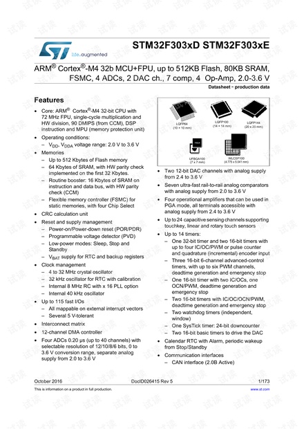
LQFP64
LQF
P100
LQFP144
UFBGA100
(10 × 10 mm)
(14 × 14 mm)
(20 x 20 mm)
(7 x 7 mm)
WLCSP100
(
4.775 x 5.041 mm
)
www.st.com

STM32F303xD STM32F303xE
2/173 DocID026415 Rev 5
– Three I
2
C Fast mode plus (1 Mbit/s) with
20 mA current sink, SMBus/PMBus,
wakeup from STOP
– Up to five USART/UARTs (ISO
7816
in
terface, LIN, IrDA, modem control)
– Up to four SPIs, 4 to 16 programmable
bit
frames, tw
o wi
th multiplexed half/full duplex
I
2
S interface
– USB 2.0 full-speed interface with LPM
support
–
Infrared transmitter
• SWD, Cortex
®
-M4 with FPU ETM, JTAG
• 96-bit unique ID
Table 1. Device summary
Reference Part number
STM32
F303xD STM32F303RD, STM32F303VD, STM32F303ZD.
STM32F303xE STM32F303RE, STM32F303VE, STM32F303ZE.

DocID026415 Rev 5 3/173
STM32F303xD STM32F303xE Contents
5
Contents
1 Introduction . . . . . . . . . . . . . . . . . . . . . . . . . . . . . . . . . . . . . . . . . . . . . . . 11
2 Description . . . . . . . . . . . . . . . . . . . . . . . . . . . . . . . . . . . . . . . . . . . . . . . . 12
3 Functional overview . . . . . . . . . . . . . . . . . . . . . . . . . . . . . . . . . . . . . . . . 16
3.1 ARM
®
Cortex
®
-M4 core with FPU with embedded Flash and SRAM . . . 16
3.2 Memory protection unit (MPU) . . . . . . . . . . . . . . . . . . . . . . . . . . . . . . . . . 16
3.3 Embedded Flash memory . . . . . . . . . . . . . . . . . . . . . . . . . . . . . . . . . . . . 16
3.4 Embedded SRAM . . . . . . . . . . . . . . . . . . . . . . . . . . . . . . . . . . . . . . . . . . . 17
3.5 Boot modes . . . . . . . . . . . . . . . . . . . . . . . . . . . . . . . . . . . . . . . . . . . . . . . 17
3.6 Cyclic redundancy check (CRC) . . . . . . . . . . . . . . . . . . . . . . . . . . . . . . . 17
3.7 Power management . . . . . . . . . . . . . . . . . . . . . . . . . . . . . . . . . . . . . . . . . 18
3.7.1 Power supply schemes . . . . . . . . . . . . . . . . . . . . . . . . . . . . . . . . . . . . . 18
3.7.2 Power supply supervisor . . . . . . . . . . . . . . . . . . . . . . . . . . . . . . . . . . . . 18
3.7.3 Voltage regulator . . . . . . . . . . . . . . . . . . . . . . . . . . . . . . . . . . . . . . . . . . 18
3.7.4 Low-power modes . . . . . . . . . . . . . . . . . . . . . . . . . . . . . . . . . . . . . . . . . 19
3.8 Interconnect matrix . . . . . . . . . . . . . . . . . . . . . . . . . . . . . . . . . . . . . . . . . . 19
3.9 Clocks and startup . . . . . . . . . . . . . . . . . . . . . . . . . . . . . . . . . . . . . . . . . . 20
3.10 General-purpose input/outputs (GPIOs) . . . . . . . . . . . . . . . . . . . . . . . . . . 22
3.11 Direct memory access (DMA) . . . . . . . . . . . . . . . . . . . . . . . . . . . . . . . . . 22
3.12 Flexible static memory controller (FSMC) . . . . . . . . . . . . . . . . . . . . . . . . 22
3.13 Interrupts and events . . . . . . . . . . . . . . . . . . . . . . . . . . . . . . . . . . . . . . . . 23
3.13.1 Nested vectored interrupt controller (NVIC) . . . . . . . . . . . . . . . . . . . . . . 23
3.14 Fast analog-to-digital converter (ADC) . . . . . . . . . . . . . . . . . . . . . . . . . . . 23
3.14.1 Temperature sensor . . . . . . . . . . . . . . . . . . . . . . . . . . . . . . . . . . . . . . . . 24
3.14.2 Internal voltage reference (V
REFINT
) . . . . . . . . . . . . . . . . . . . . . . . . . . . 24
3.14.3 V
BAT
battery voltage monitoring . . . . . . . . . . . . . . . . . . . . . . . . . . . . . . . 24
3.14.4 OPAMP reference voltage (VREFOPAMP) . . . . . . . . . . . . . . . . . . . . . . 24
3.15 Digital-to-analog converter (DAC) . . . . . . . . . . . . . . . . . . . . . . . . . . . . . . 24
3.16 Operational amplifier (OPAMP) . . . . . . . . . . . . . . . . . . . . . . . . . . . . . . . . 25
3.17 Ultra-fast comparators (COMP) . . . . . . . . . . . . . . . . . . . . . . . . . . . . . . . . 25
3.18 Timers and watchdogs . . . . . . . . . . . . . . . . . . . . . . . . . . . . . . . . . . . . . . . 25

Contents STM32F303xD STM32F303xE
4/173 DocID026415 Rev 5
3.18.1 Advanced timers (TIM1, TIM8, TIM20) . . . . . . . . . . . . . . . . . . . . . . . . . 26
3.18.2 General-purpose timers (TIM2, TIM3, TIM4, TIM15, TIM16, TIM17) . . 26
3.18.3 Basic timers (TIM6, TIM7) . . . . . . . . . . . . . . . . . . . . . . . . . . . . . . . . . . . 27
3.18.4 Independent watchdog (IWDG) . . . . . . . . . . . . . . . . . . . . . . . . . . . . . . . 27
3.18.5 Window watchdog (WWDG) . . . . . . . . . . . . . . . . . . . . . . . . . . . . . . . . . 27
3.18.6 SysTick timer . . . . . . . . . . . . . . . . . . . . . . . . . . . . . . . . . . . . . . . . . . . . . 28
3.19 Real-time clock (RTC) and backup registers . . . . . . . . . . . . . . . . . . . . . . 28
3.20 Inter-integrated circuit interface (I
2
C) . . . . . . . . . . . . . . . . . . . . . . . . . . . . 28
3.21 Universal synchronous/asynchronous receiver transmitter (USART) . . . 29
3.22 Universal asynchronous receiver transmitter (UART) . . . . . . . . . . . . . . . 30
3.23 Serial peripheral interface (SPI)/Inter-integrated sound interfaces (I
2
S) . 30
3.24 Controller area network (CAN) . . . . . . . . . . . . . . . . . . . . . . . . . . . . . . . . . 31
3.25 Universal serial bus (USB) . . . . . . . . . . . . . . . . . . . . . . . . . . . . . . . . . . . . 31
3.26 Infrared transmitter . . . . . . . . . . . . . . . . . . . . . . . . . . . . . . . . . . . . . . . . . . 31
3.27 Touch sensing controller (TSC) . . . . . . . . . . . . . . . . . . . . . . . . . . . . . . . . 32
3.28 Development support . . . . . . . . . . . . . . . . . . . . . . . . . . . . . . . . . . . . . . . . 33
3.28.1 Serial wire JTAG debug port (SWJ-DP) . . . . . . . . . . . . . . . . . . . . . . . . . 33
3.28.2 Embedded Trace Macrocell . . . . . . . . . . . . . . . . . . . . . . . . . . . . . . . . . . 33
4 Pinout and pin description . . . . . . . . . . . . . . . . . . . . . . . . . . . . . . . . . . . 35
5 Memory mapping . . . . . . . . . . . . . . . . . . . . . . . . . . . . . . . . . . . . . . . . . . . 64
6 Electrical characteristics . . . . . . . . . . . . . . . . . . . . . . . . . . . . . . . . . . . . 68
6.1 Parameter conditions . . . . . . . . . . . . . . . . . . . . . . . . . . . . . . . . . . . . . . . . 68
6.1.1 Minimum and maximum values . . . . . . . . . . . . . . . . . . . . . . . . . . . . . . . 68
6.1.2 Typical values . . . . . . . . . . . . . . . . . . . . . . . . . . . . . . . . . . . . . . . . . . . . 68
6.1.3 Typical curves . . . . . . . . . . . . . . . . . . . . . . . . . . . . . . . . . . . . . . . . . . . . 68
6.1.4 Loading capacitor . . . . . . . . . . . . . . . . . . . . . . . . . . . . . . . . . . . . . . . . . 68
6.1.5 Pin input voltage . . . . . . . . . . . . . . . . . . . . . . . . . . . . . . . . . . . . . . . . . . 68
6.1.6 Power supply scheme . . . . . . . . . . . . . . . . . . . . . . . . . . . . . . . . . . . . . . 69
6.1.7 Current consumption measurement . . . . . . . . . . . . . . . . . . . . . . . . . . . 70
6.2 Absolute maximum ratings . . . . . . . . . . . . . . . . . . . . . . . . . . . . . . . . . . . . 70
6.3 Operating conditions . . . . . . . . . . . . . . . . . . . . . . . . . . . . . . . . . . . . . . . . 72
6.3.1 General operating conditions . . . . . . . . . . . . . . . . . . . . . . . . . . . . . . . . . 72
6.3.2 Operating conditions at power-up / power-down . . . . . . . . . . . . . . . . . . 73

DocID026415 Rev 5 5/173
STM32F303xD STM32F303xE Contents
5
6.3.3 Embedded reset and power control block characteristics . . . . . . . . . . . 73
6.3.4 Embedded reference voltage . . . . . . . . . . . . . . . . . . . . . . . . . . . . . . . . . 74
6.3.5 Supply current characteristics . . . . . . . . . . . . . . . . . . . . . . . . . . . . . . . . 74
6.3.6 Wakeup time from low-power mode . . . . . . . . . . . . . . . . . . . . . . . . . . . 87
6.3.7 External clock source characteristics . . . . . . . . . . . . . . . . . . . . . . . . . . . 88
6.3.8 Internal clock source characteristics . . . . . . . . . . . . . . . . . . . . . . . . . . . 92
6.3.9 PLL characteristics . . . . . . . . . . . . . . . . . . . . . . . . . . . . . . . . . . . . . . . . 93
6.3.10 Memory characteristics . . . . . . . . . . . . . . . . . . . . . . . . . . . . . . . . . . . . . 94
6.3.11 FSMC characteristics . . . . . . . . . . . . . . . . . . . . . . . . . . . . . . . . . . . . . . . 94
6.3.12 EMC characteristics . . . . . . . . . . . . . . . . . . . . . . . . . . . . . . . . . . . . . . . 115
6.3.13 Electrical sensitivity characteristics . . . . . . . . . . . . . . . . . . . . . . . . . . . 116
6.3.14 I/O current injection characteristics . . . . . . . . . . . . . . . . . . . . . . . . . . . 117
6.3.15 I/O port characteristics . . . . . . . . . . . . . . . . . . . . . . . . . . . . . . . . . . . . . 118
6.3.16 NRST pin characteristics . . . . . . . . . . . . . . . . . . . . . . . . . . . . . . . . . . . 123
6.3.17 Timer characteristics . . . . . . . . . . . . . . . . . . . . . . . . . . . . . . . . . . . . . . 124
6.3.18 Communications interfaces . . . . . . . . . . . . . . . . . . . . . . . . . . . . . . . . . 125
6.3.19 ADC characteristics . . . . . . . . . . . . . . . . . . . . . . . . . . . . . . . . . . . . . . . 132
6.3.20 DAC electrical specifications . . . . . . . . . . . . . . . . . . . . . . . . . . . . . . . . 144
6.3.21 Comparator characteristics . . . . . . . . . . . . . . . . . . . . . . . . . . . . . . . . . 146
6.3.22 Operational amplifier characteristics . . . . . . . . . . . . . . . . . . . . . . . . . . 148
6.3.23 Temperature sensor characteristics . . . . . . . . . . . . . . . . . . . . . . . . . . . 150
6.3.24 V
BAT
monitoring characteristics . . . . . . . . . . . . . . . . . . . . . . . . . . . . . . 151
7 Package information . . . . . . . . . . . . . . . . . . . . . . . . . . . . . . . . . . . . . . . 152
7.1 Package mechanical data . . . . . . . . . . . . . . . . . . . . . . . . . . . . . . . . . . . 152
7.2 LQFP144 package information . . . . . . . . . . . . . . . . . . . . . . . . . . . . . . . . 152
7.3 UFBGA100 package information . . . . . . . . . . . . . . . . . . . . . . . . . . . . . . 156
7.4 LQFP100 package information . . . . . . . . . . . . . . . . . . . . . . . . . . . . . . . . 159
7.5 WLCSP100 package information . . . . . . . . . . . . . . . . . . . . . . . . . . . . . . 162
7.6 LQFP64 package information . . . . . . . . . . . . . . . . . . . . . . . . . . . . . . . . . 165
7.7 Thermal characteristics . . . . . . . . . . . . . . . . . . . . . . . . . . . . . . . . . . . . . 168
7.7.1 Reference document . . . . . . . . . . . . . . . . . . . . . . . . . . . . . . . . . . . . . . 168
7.7.2 Selecting the product temperature range . . . . . . . . . . . . . . . . . . . . . . 168
8 Part numbering . . . . . . . . . . . . . . . . . . . . . . . . . . . . . . . . . . . . . . . . . . . 171
9 Revision history . . . . . . . . . . . . . . . . . . . . . . . . . . . . . . . . . . . . . . . . . . 172
剩余172页未读,继续阅读


安全验证
文档复制为VIP权益,开通VIP直接复制

评论0