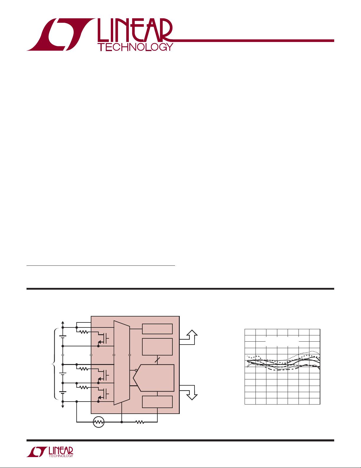
没有合适的资源?快使用搜索试试~ 我知道了~
首页LTC6802技术手册
LTC6802技术手册
需积分: 20 106 浏览量
更新于2023-03-16
评论 1
收藏 329KB PDF 举报
LTC6802技术手册,用于电动汽车的学电池的管理系统,是一款集成度很高,精度很高的芯片。
资源详情
资源评论
资源推荐

LTC6802-1
1
68021fa
TYPICAL APPLICATION
DESCRIPTION
Multicell
Battery Stack Monitor
The LTC
®
6802-1 is a complete battery monitoring IC that
includes a 12-bit ADC, a precision voltage reference, a
high voltage input multiplexer and a serial interface. Each
LTC6802-1 can measure up to 12 series connected bat-
tery cells with an input common mode voltage up to 60V.
In addition, multiple LTC6802-1 devices can be placed in
series to monitor the voltage of each cell in a long battery
string. The unique level-shifting serial interface allows the
serial ports of these devices to be daisy-chained without
optocouplers or isolators.
When multiple LTC6802-1 devices are connected in series
they can operate simultaneously, permitting all cell voltages
in the stack to be measured within 13ms.
To minimize power, the LTC6802-1 offers a measure mode,
which simply monitors each cell for overvoltage and un-
dervoltage conditions. A standby mode is also provided.
Each cell input has an associated MOSFET switch for
discharging overcharged cells.
For large battery stack applications requiring individually
addressable serial communications, see the LTC6802-2.
FEATURES
APPLICATIONS
n
Measures up to 12 Li-Ion Cells in Series (60V Max)
n
Stackable Architecture Enables >1000V Systems
n
0.25% Maximum Total Measurement Error
n
13ms to Measure All Cells in a System
n
Cell Balancing:
On-Chip Passive Cell Balancing Switches
Provision for Off-Chip Passive Balancing
n
Two Thermistor Inputs Plus On-Board
Temperature Sensor
n
1MHz Daisy-Chainable Serial Interface
n
High EMI Immunity
n
Delta Sigma Converter with Built-In Noise Filter
n
Open Wire Connection Fault Detection
n
Low Power Modes
n
44-Lead SSOP Package
n
Electric and Hybrid Electric Vehicles
n
High Power Portable Equipment
n
Backup Battery Systems
n
High Voltage Data Acquisition Systems
MUX
DIE TEMP
12-CELL
BATTERY
STRING
NEXT 12-CELL
PACK ABOVE
NEXT 12-CELL
PACK BELOW
V
+
V
–
100k NTC
100k
EXTERNAL
TEMP
SERIAL DATA
TO LTC6802-1
ABOVE
SERIAL DATA
TO LTC6802-1
BELOW
LTC6802-1
68021 TA01a
VOLTAGE
REFERENCE
REGISTERS
AND
CONTROL
12-BIT
Δ∑ ADC
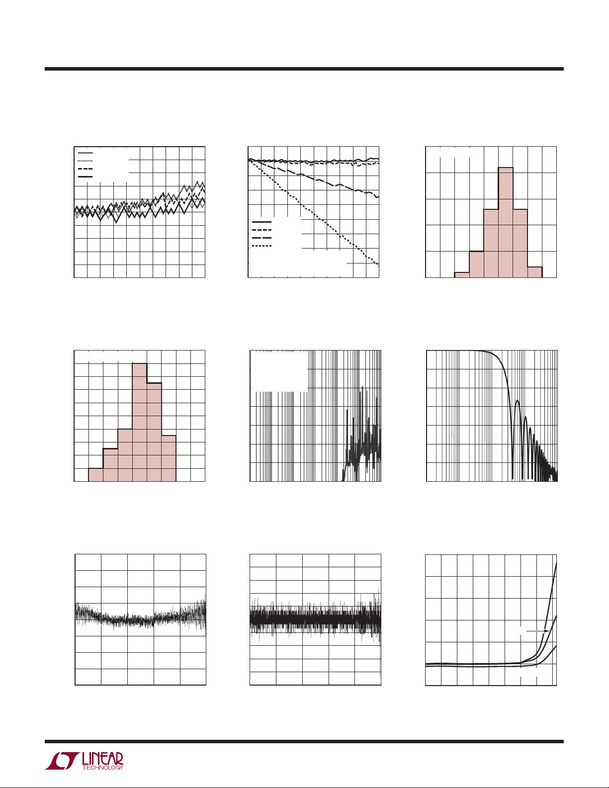
MEASUREMENT ERROR (%)
TEMPERATURE (°C)
125–50
0.30
–0.30
–25 0 25 50 75 100
–0.20
–0.25
–0.10
0.10
0
0.20
–0.15
–0.05
0.15
0.05
0.25
7 REPRESENTATIVE
UNITS
68021 TA01b
Measurement Error Over
Extended Temperature
L, LT, LTC, LTM, Linear Technology and the Linear logo are registered trademarks of Linear
Technology Corporation. All other trademarks are the property of their respective owners.

LTC6802-1
2
68021fa
PIN CONFIGURATIONABSOLUTE MAXIMUM RATINGS
Total Supply Voltage (V
+
to V
–
) .................................60V
Input Voltage (Relative to V
–
)
C1 ............................................................ –0.3V to 9V
C12 .......................................... V
+
– 0.6V to V
+
+ 0.3V
Cn (Note 5) ......................... –0.3V to min (9 • n, 60V)
Sn (Note 5) ......................... –0.3V to min (9 • n, 60V)
CSBO, SCKO, SDOI .................. V
+
– 0.6V to V
+
+ 0.3V
All other pins ........................................... –0.3V to 7V
Voltage Between Inputs
Cn to Cn-1 ................................................ –0.3V to 9V
Sn to Cn-1 ................................................ –0.3V to 9V
C12 to C8 ............................................... –0.3V to 25V
C8 to C4 ................................................. –0.3V to 25V
C4 to V
–
................................................. –0.3V to 25V
Operating Temperature Range .................–40°C to 85°C
Specified Temperature Range ..................–40°C to 85°C
Junction Temperature ........................................... 150°C
Storage Temperature Range .................. –65°C to 150°C
*n = 1 to 12
(Note 1)
1
2
3
4
5
6
7
8
9
10
11
12
13
14
15
16
17
18
19
20
21
22
TOP VIEW
G PACKAGE
44-LEAD PLASTIC SSOP
44
43
42
41
40
39
38
37
36
35
34
33
32
31
30
29
28
27
26
25
24
23
CSBO
SDOI
SCKO
V
+
C12
S12
C11
S11
C10
S10
C9
S9
C8
S8
C7
S7
C6
S6
C5
S5
C4
S4
CSBI
SDO
SDI
SCKI
V
MODE
GPIO2
GPIO1
WDTB
MMB
TOS
V
REG
V
REF
V
TEMP2
V
TEMP1
NC
V
–
S1
C1
S2
C2
S3
C3
T
JMAX
= 150°C, θ
JA
= 70°C/W
ORDER INFORMATION
LEAD FREE FINISH TAPE AND REEL PART MARKING PACKAGE DESCRIPTION TEMPERATURE RANGE
LTC6802IG-1#PBF LTC6802IG-1#TRPBF LTC6802G-1 44-Lead Plastic SSOP –40°C to 85°C
Consult LTC Marketing for parts specified with wider operating temperature ranges.
Consult LTC Marketing for information on non-standard lead based finish parts.
For more information on lead free part marking, go to:
http://www.linear.com/leadfree/
For more information on tape and reel specifications, go to:
http://www.linear.com/tapeandreel/

LTC6802-1
3
68021fa
ELECTRICAL CHARACTERISTICS
The l denotes the specifications which apply over the full operating
temperature range, otherwise specifications are at T
A
= 25°C. V
+
= 43.2V, V
–
= 0V, unless otherwise noted.
SYMBOL PARAMETER CONDITIONS MIN TYP MAX UNITS
DC Specifications
V
ACC
Measurement Resolution Quantization of the ADC
l
1.5 mV/Bit
ADC Offset Voltage (Note 2)
l
–0.5 0.5 mV
ADC Gain Error (Note 2)
l
–0.12
–0.22
0.12
0.22
%
%
V
ERR
Total Measurement Error (Note 4)
V
CELL
= 0V
V
CELL
= 2.3V
V
CELL
= 2.3V
V
CELL
= 3.6V
V
CELL
= 3.6V
V
CELL
= 4.2V
V
CELL
= 4.2V
V
CELL
= 4.6V
V
TEMP
= 2.3V
V
TEMP
= 3.6V
V
TEMP
= 4.2V
l
l
l
l
l
l
–2.8
–5.1
–4.3
–7.9
–5
–9.2
–5.1
–7.9
–9.2
0.8
±8
2.8
5.1
4.3
7.9
5
9.2
5.1
7.9
9.2
mV
mV
mV
mV
mV
mV
mV
mV
mV
mV
mV
V
CELL
Cell Voltage Range Full Scale Voltage Range 5 V
V
CM
Common Mode Voltage Range Measured
Relative to V
–
Range of Inputs CN for <0.25% Gain Error, N = 3 to 11
Range of Input C3 for <1% Gain Error
Range of Input C2 for <0.25% Gain Error
Range of Input C1 for <0.25% Gain Error
l
l
l
l
3.7
1.8
1.2
0
5 • N
15
10
5
V
V
V
V
Overvoltage (OV) Detection Level Programmed for 4.2V
l
4.182 4.200 4.218 V
Undervoltage (UV) Detection Level Programmed for 2.3V
l
2.290 2.300 2.310 V
Die Temperature Measurement Error Error in Measurement at 125°C 3 °C
V
REF
Reference Pin Voltage R
LOAD
= 100k to V
–
l
3.020
3.015
3.065
3.065
3.110
3.115
V
V
Reference Voltage Temperature Coefficient 8 ppm/°C
Reference Voltage Thermal Hysteresis 25°C to 85°C and 25°C to –40°C 100 ppm
Reference Voltage Long Term Drift 60 ppm/√khr
V
REG
Regulator Pin Voltage 10 < V
+
< 50, No Load
I
LOAD
= 4mA
l
l
4.5
4.1
5.0
4.8
5.5 V
V
Regulator Pin Short Circuit Current Limit
l
58 mA
V
S
Supply Voltage, V
+
Relative to V
–
V
ERR
Specifications Met
Timing Specifications Met
l
l
10
4
50
50
V
V
I
B
Input Bias Current In/Out of Pins C1 Thru C12
When Measuring Cells
When Not Measuring Cells
l
–10
1
10 μA
nA
I
S
Supply Current, Active Current Into the V
+
Pin when Measuring Voltages
with the ADC
l
0.8 1.1
1.2
mA
mA
I
M
Supply Current, Monitor Mode Average Current Into the V
+
Pin While Monitoring
for UV and OV Conditions
Continuous Monitoring (CDC = 2)
Monitor Every 130ms (CDC = 5)
Monitor Every 500ms (CDC = 6)
Monitor Every 2s (CDC = 7)
800
225
150
100
μA
μA
μA
μA
I
QS
Supply Current, Idle Current into the V
+
Pin When Idle
All Serial Port Pins at Logic ‘1’
l
35
30
60 80
85
μA
μA
I
CS
Supply Current, Serial I/O All Serial Port Pins at Logic ‘0’ V
MODE
= 0, This
Current is Added to I
S
or I
QS
l
3 4.5 mA

LTC6802-1
4
68021fa
Note 1: Stresses beyond those listed under Absolute Maximum Ratings
may cause permanent damage to the device. Exposure to any Absolute
Maximum Rating condition for extended periods may affect device
reliability and lifetime.
Note 2: The ADC specifications are guaranteed by the Total Measurement
Error (V
ERR
) specification.
SYMBOL PARAMETER CONDITIONS MIN TYP MAX UNITS
Discharge Switch On-Resistance V
CELL
> 3V (Note 3)
l
10 20 Ω
Temperature Range
l
–40 85 °C
Thermal Shutdown Temperature 145 °C
Thermal Shutdown Hysteresis 5°C
Voltage Mode Timing Specifications
t
CYCLE
Measurement Cycle Time Time Required to Measure 11 or 12 Cells
Time Required to Measure Up to 10 Cells
Time Required to Measure 1 Cell
l
l
11
9.2
1
13
11
1.2
16
13.5
1.5
ms
ms
ms
t
1
SDI Valid to SCKI Rising Setup
l
10 ns
t
2
SDI Valid to SCKI Rising Hold
l
250 ns
t
3
SCKI Low
l
400 ns
t
4
SCKI High
l
400 ns
t
5
CSBI Pulse Width
l
400 ns
t
6
SCKI Rising to CSBI Rising
l
100 ns
t
7
CSBI Falling to SCKI Rising
l
100 ns
t
8
SCKI Falling to SDO Valid
l
250 ns
Clock Frequency
l
1 MHz
Watchdog Timer Time Out Period
l
1 2.5 s
Timing Specifications
t
PD1
CSBI to CSBO C
CSBO
= 150pF
l
600 ns
t
PD2
SCKI to SCKO C
SCKO
= 150pF
l
300 ns
t
PD3
SDI to SDOI Write Delay C
SDOI
= 150pF
l
300 ns
t
PD4
SDOI to SDI Read Delay C
SDO
= 150pF
l
300 ns
Voltage Mode Digital I/O Specifications
V
IH
Digital Input Voltage High Pins SCKI, SDI, and CSBI
l
2V
V
IL
Digital Input Voltage Low Pins SCKI, SDI, and CSBI
l
0.8 V
V
OL
Digital Output Voltage Low Pin SDO; Sinking 500μA
l
0.3 V
Current Mode Digital I/O Specifications
I
IH1
Digital Input Current High Pins CSBI, SCKI, and SDI (Write)
l
10 μA
I
IL1
Digital Input Current Low Pins CSBI, SCKI, and SDI (Write)
l
1000 μA
I
IH2
Digital Input Current High Pin SDOI (Read)
l
–1000 μA
I
IL2
Digital Input Current Low Pin SDOI (Read)
l
–10 μA
I
OH1
Digital Output Current High Pins CSBO, SCKO, and SDOI (Write)
l
310 μA
I
OL1
Digital Output Current Low Pins CSBO, SCKO, and SDOI (Write)
l
1000 1200 1650 μA
I
OH2
Digital Output Current High Pin SDI (Read)
l
–1650 –1200 –1000 μA
I
OL2
Digital Output Current Low Pin SDI (Read)
l
–10 –3 0 μA
ELECTRICAL CHARACTERISTICS
The l denotes the specifications which apply over the full operating
temperature range, otherwise specifications are at T
A
= 25°C. V
+
= 43.2V, V
–
= 0V, unless otherwise noted.
Note 3: Due to the contact resistance of the production tester, this
specification is tested to relaxed limits. The 20Ω limit is guaranteed by
design.
Note 4: V
CELL
refers to the voltage applied across the following pin
combinations: Cn to Cn-1 for n = 2 to 12, C1 to V
–
. V
TEMP
refers to the
voltage applied from V
TEMP1
or V
TEMP2
to V
–
.
Note 5: These absolute maximum ratings apply provided that the voltage
between inputs do not exceed their absolute maximum ratings.

LTC6802-1
5
68021fa
TYPICAL PERFORMANCE CHARACTERISTICS
Cell Measurement Total
Unadjusted Error
vs Input Resistance
Cell Measurement Total
Unadjusted Error
CELL VOLTAGE (V)
0
TOTAL UNADJUSTED ERROR (mV)
10
–8
8
4
0
–4
6
2
–2
–6
–10
2.5 4.51.5 3.5
68021 G01
5.02.0 4.01.0 3.00.5
T
A
= –40°C
T
A
= 25°C
T
A
= 85°C
T
A
= 125°C
CELL VOLTAGE (V)
0
TOTAL UNADJUSTED ERROR (mV)
10
0
–20
–40
–60
–10
–30
–50
–70
–80
2.5 4.51.5 3.5
68021 G02
5.02.0 4.01.0 3.00.5
R
S
= 1k
R
S
= 2k
R
S
= 5k
R
S
= 10k
R
S
IN SERIES WITH CN AND CN-1
NO EXTERNAL CAPACITANCE ON
CN AND CN-1
Measurement Gain Error
Hysteresis
Measurement Gain Error
Hysteresis
CHANGE IN GAIN ERROR (ppm)
–250
NUMBER OF UNITS
25
20
15
10
5
0
–50 150–150 50
68021 G03
200–100 100–200 0
T
A
= 85°C TO 25°C
CHANGE IN GAIN ERROR (ppm)
–250
NUMBER OF UNITS
20
16
12
8
4
18
14
10
6
2
0
–50 150–150 50
68021 G04
200–100 100–200 0
T
A
= –45°C TO 25°C
ADC Normal Mode Rejection
vs Frequency
Cell Measurement Common Mode
Rejection
0
–10
–30
–50
–20
–40
–60
–70
FREQUENCY (Hz)
REJECTION (db)
68021 G06
10 10k 100k1k100
0
–10
–30
–50
–20
–40
–60
–70
FREQUENCY (Hz)
REJECTION (db)
68021 G05
10 10k 10M1M100k1k100
V
CM(IN)
= 5V
P-P
72dB REJECTION
CORRESPONDS TO
LESS THAN 1 BIT
AT ADC OUTPUT
ADC INL ADC DNL
INPUT (V)
0
INL (BITS)
2.0
1.5
0.5
1.0
0
–1.0
–0.5
–1.5
–2.0
12 4
68021 G07
53
INPUT (V)
0
DNL (BITS)
1.0
0.8
0.2
0.4
0.6
0
–0.6
–0.4
–0.2
–0.8
–1.0
12 4
68021 G08
53
Cell Input Bias Current in Standby
TEMPERATURE (°C)
–40
C PIN BIAS CURRENT (nA)
50
40
30
20
10
–10
0
20–20 400 80 10060
68021 G09
120
C2 TO C11
C1
C12
剩余37页未读,继续阅读


安全验证
文档复制为VIP权益,开通VIP直接复制

评论0