没有合适的资源?快使用搜索试试~ 我知道了~
首页EFM8LB1系列芯片详细资料
资源详情
资源评论
资源推荐
EFM8 Laser Bee Family
EFM8LB1 Reference Manual
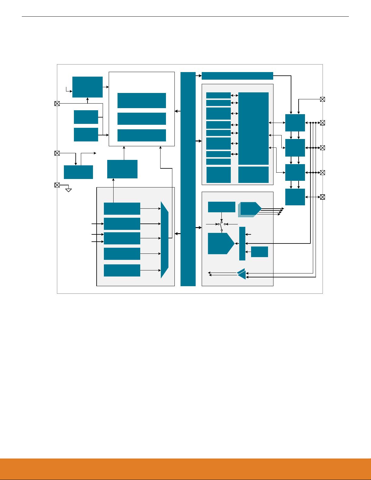
The EFM8LB1, part of the Laser Bee family of MCUs, is a per-
formance line of 8-bit microcontrollers with a comprehensive ana-
log and digital feature set in small packages.
These devices offer state-of-the-art performance by integrating 14-bit ADC, internal
calibrated temperature sensor (±3 °C), and up to four 12-bit DACs into small packages,
making them ideal for the most stringent analog requirement applications. With an effi-
cient, pipelined 8051 core with maximum operating frequency at 72 MHz, various com-
munication interfaces, and four channels of configurable logic, the EFM8LB1 family is
optimal for many embedded applications.
EFM8LB1 applications include the following:
Core / Memory Clock Management
KEY FEATURES
• Pipelined 8-bit 8051 MCU Core with
72 MHz operating frequency
• Up to 29 multifunction I/O pins
• One 14-bit, 900 ksps ADC
• Up to four 12-bit DACs with
synchronization and PWM capabilities
• Two low-current analog comparators with
built-in reference DACs
• Internal calibrated temperature sensor
(±3 °C)
• Internal 72 MHz and 24.5 MHz oscillators
accurate to ±2%
• Four channels of Configurable Logic
• 6-channel PWM / PCA
• Six 16-bit general-purpose timers
Energy Management
Flash Program
Memory
(up to 64 KB)
RAM Memory
(up to 4352 bytes)
Debug Interface
with C2
External
Oscillator
Low Frequency
RC Oscillator
8-bit SFR bus
High Frequency
72 MHz RC
Oscillator
High Frequency
24.5 MHz RC
Oscillator
Internal LDO
Regulator
Power-On Reset
Serial Interfaces I/O Ports Timers and Triggers Analog Interfaces Security
Timers
2 x UART
I
2
C / SMBus
SPI
High-Speed
I2C Slave
External
Interrupts
General
Purpose I/O
Pin Wakeup
Up to 4 x
4 x Configurable Logic Units
Voltage DAC
2 x
16-bit CRC
Comparators
Internal
Voltage
Reference
Lowest power mode with peripheral operational:
Normal Idle Suspend Snooze Shutdown
silabs.com | Smart. Connected. Energy-friendly. Preliminary Rev. 0.3
This information applies to a product under development. Its characteristics and specifications are subject to change without notice.
• Optical network modules
• Precision instrumentation
• Industrial control and automation
• Smart sensors
CIP-51 8051 Core
(72 MHz)
Brown-Out Detector
PCA/PWM
Pin Reset ADC
0/1/2/5
Watchdog
Timer
Timer 3/4
+
-
EFM8LB1 Reference Manual
System Overview
1. System Overview
1.1 Introduction
C2CK/RSTb
C2D
Debug /
Programming
Hardware
Reset
Power-On
Reset
Port I/O Configuration
Digital Peripherals
UART0
UART1
Timers 0,
1, 2, 3, 4, 5
VIO
Supply
Monitor
Power
Net
6-ch PCA
I2C Slave
I2C /
SMBus
SPI
CRC
Priority
Crossbar
Decoder
Drivers
Port 1
Drivers
P1.n
GND
Voltage
Regulator
Watchdog
Timer
System Clock
Configuration
Low Freq.
Oscillator
SFR
Bus
Config.
Logic
Units (4)
Internal
Reference
Crossbar
Control
4 12-bit
DACs
Port 2
Drivers
Port 3
Drivers
P2.n
P3.n
EXTCLK
XTAL1
XTAL2
CMOS Clock
Input
External Crystal /
RC Oscillator
72 MHz 2%
Oscillator
24.5 MHz 2%
Oscillator
14/12/10-
bit ADC
+
-
VDD
Temp
Sensor
2 Comparators
Figure 1.1. Detailed EFM8LB1 Block Diagram
silabs.com | Smart. Connected. Energy-friendly. Preliminary Rev. 0.3 | 1
CIP-51 8051 Controller
Core
64 KB ISP Flash
Program Memory
256 Byte SRAM
4096 Byte XRAM
Port 0
P0.n
VDD
Independent
SYSCLK
Analog Peripherals
VDD
VREF
EFM8LB1 Reference Manual
System Overview
1.2 Power
All internal circuitry draws power from the VDD supply pin. External I/O pins are powered from the VIO supply voltage (or VDD on devi-
ces without a separate VIO connection), while most of the internal circuitry is supplied by an on-chip LDO regulator. Control over the
device power can be achieved by enabling/disabling individual peripherals as needed. Each analog peripheral can be disabled when
not in use and placed in low power mode. Digital peripherals, such as timers and serial buses, have their clocks gated off and draw little
power when they are not in use.
Table 1.1. Power Modes
Power Mode Details Mode Entry Wake-Up Sources
Normal Core and all peripherals clocked and fully operational
Idle • Core halted Set IDLE bit in PCON0 Any interrupt
• All peripherals clocked and fully operational
• Code resumes execution on wake event
Suspend • Core and peripheral clocks halted
• HFOSC0 and HFOSC1 oscillators stopped
• Regulator in normal bias mode for fast wake
• Timer 3 and 4 may clock from LFOSC0
• Code resumes execution on wake event
1. Switch SYSCLK to
HFOSC0
2. Set SUSPEND bit in
PCON1
• Timer 4 Event
• SPI0 Activity
• I2C0 Slave Activity
• Port Match Event
• Comparator 0 Falling
Edge
• CLUn Interrupt-Enabled
Event
Stop • All internal power nets shut down
• Pins retain state
• Exit on any reset source
Snooze • Core and peripheral clocks halted
• HFOSC0 and HFOSC1 oscillators stopped
• Regulator in low bias current mode for energy sav-
ings
• Timer 3 and 4 may clock from LFOSC0
• Code resumes execution on wake event
1. Clear STOPCF bit in
REG0CN
2. Set STOP bit in
PCON0
1. Switch SYSCLK to
HFOSC0
2. Set SNOOZE bit in
PCON1
Any reset source
• Timer 4 Event
• SPI0 Activity
• I2C0 Slave Activity
• Port Match Event
• Comparator 0 Falling
Edge
• CLUn Interrupt-Enabled
Event
Shutdown • All internal power nets shut down
• Pins retain state
• Exit on pin or power-on reset
1. Set STOPCF bit in
REG0CN
2. Set STOP bit in
PCON0
• RSTb pin reset
• Power-on reset
1.3 I/O
Digital and analog resources are externally available on the device’s multi-purpose I/O pins. Port pins P0.0-P2.3 can be defined as gen-
eral-purpose I/O (GPIO), assigned to one of the internal digital resources through the crossbar or dedicated channels, or assigned to an
analog function. Port pins P2.4 to P3.7 can be used as GPIO. Additionally, the C2 Interface Data signal (C2D) is shared with P3.0 or
P3.7, depending on the package option.
The port control block offers the following features:
• Up to 29 multi-functions I/O pins, supporting digital and analog functions.
• Flexible priority crossbar decoder for digital peripheral assignment.
• Two drive strength settings for each port.
• State retention feature allows pins to retain configuration through most reset sources.
• Two direct-pin interrupt sources with dedicated interrupt vectors (INT0 and INT1).
• Up to 24 direct-pin interrupt sources with shared interrupt vector (Port Match).
silabs.com | Smart. Connected. Energy-friendly. Preliminary Rev. 0.3 | 2
EFM8LB1 Reference Manual
System Overview
1.4 Clocking
The CPU core and peripheral subsystem may be clocked by both internal and external oscillator resources. By default, the system
clock comes up running from the 24.5 MHz oscillator divided by 8.
The clock control system offers the following features:
• Provides clock to core and peripherals.
• 24.5 MHz internal oscillator (HFOSC0), accurate to ±2% over supply and temperature corners.
• 72 MHz internal oscillator (HFOSC1), accurate to ±2% over supply and temperature corners.
• 80 kHz low-frequency oscillator (LFOSC0).
• External RC, CMOS, and high-frequency crystal clock options (EXTCLK).
• Clock divider with eight settings for flexible clock scaling:
• Divide the selected clock source by 1, 2, 4, 8, 16, 32, 64, or 128.
• HFOSC0 and HFOSC1 include 1.5x pre-scalers for further flexibility.
1.5 Counters/Timers and PWM
Programmable Counter Array (PCA0)
The programmable counter array (PCA) provides multiple channels of enhanced timer and PWM functionality while requiring less CPU
intervention than standard counter/timers. The PCA consists of a dedicated 16-bit counter/timer and one 16-bit capture/compare mod-
ule for each channel. The counter/timer is driven by a programmable timebase that has flexible external and internal clocking options.
Each capture/compare module may be configured to operate independently in one of five modes: Edge-Triggered Capture, Software
Timer, High-Speed Output, Frequency Output, or Pulse-Width Modulated (PWM) Output. Each capture/compare module has its own
associated I/O line (CEXn) which is routed through the crossbar to port I/O when enabled.
• 16-bit time base
• Programmable clock divisor and clock source selection
• Up to six independently-configurable channels
• 8, 9, 10, 11 and 16-bit PWM modes (center or edge-aligned operation)
• Output polarity control
• Frequency output mode
• Capture on rising, falling or any edge
• Compare function for arbitrary waveform generation
• Software timer (internal compare) mode
• Can accept hardware “kill” signal from comparator 0 or comparator 1
silabs.com | Smart. Connected. Energy-friendly. Preliminary Rev. 0.3 | 3
EFM8LB1 Reference Manual
System Overview
Timers (Timer 0, Timer 1, Timer 2, Timer 3, Timer 4, and Timer 5)
Several counter/timers are included in the device: two are 16-bit counter/timers compatible with those found in the standard 8051, and
the rest are 16-bit auto-reload timers for timing peripherals or for general purpose use. These timers can be used to measure time inter-
vals, count external events and generate periodic interrupt requests. Timer 0 and Timer 1 are nearly identical and have four primary
modes of operation. The other timers offer both 16-bit and split 8-bit timer functionality with auto-reload and capture capabilities.
Timer 0 and Timer 1 include the following features:
• Standard 8051 timers, supporting backwards-compatibility with firmware and hardware.
• Clock sources include SYSCLK, SYSCLK divided by 12, 4, or 48, the External Clock divided by 8, or an external pin.
• 8-bit auto-reload counter/timer mode
• 13-bit counter/timer mode
• 16-bit counter/timer mode
• Dual 8-bit counter/timer mode (Timer 0)
Timer 2, Timer 3, Timer 4, and Timer 5 are 16-bit timers including the following features:
• Clock sources for all timers include SYSCLK, SYSCLK divided by 12, or the External Clock divided by 8
• LFOSC0 divided by 8 may be used to clock Timer 3 and Timer 4 in active or suspend/snooze power modes
• Timer 4 is a low-power wake source, and can be chained together with Timer 3
• 16-bit auto-reload timer mode
• Dual 8-bit auto-reload timer mode
• External pin capture
• LFOSC0 capture
• Comparator 0 capture
• Configurable Logic output capture
Watchdog Timer (WDT0)
The device includes a programmable watchdog timer (WDT) running off the low-frequency oscillator. A WDT overflow forces the MCU
into the reset state. To prevent the reset, the WDT must be restarted by application software before overflow. If the system experiences
a software or hardware malfunction preventing the software from restarting the WDT, the WDT overflows and causes a reset. Following
a reset, the WDT is automatically enabled and running with the default maximum time interval. If needed, the WDT can be disabled by
system software or locked on to prevent accidental disabling. Once locked, the WDT cannot be disabled until the next system reset.
The state of the RST pin is unaffected by this reset.
The Watchdog Timer has the following features:
• Programmable timeout interval
• Runs from the low-frequency oscillator
• Lock-out feature to prevent any modification until a system reset
1.6 Communications and Other Digital Peripherals
Universal Asynchronous Receiver/Transmitter (UART0)
UART0 is an asynchronous, full duplex serial port offering modes 1 and 3 of the standard 8051 UART. Enhanced baud rate support
allows a wide range of clock sources to generate standard baud rates. Received data buffering allows UART0 to start reception of a
second incoming data byte before software has finished reading the previous data byte.
The UART module provides the following features:
• Asynchronous transmissions and receptions.
• Baud rates up to SYSCLK/2 (transmit) or SYSCLK/8 (receive).
• 8- or 9-bit data.
• Automatic start and stop generation.
• Single-byte buffer on transmit and receive.
silabs.com | Smart. Connected. Energy-friendly. Preliminary Rev. 0.3 | 4
剩余391页未读,继续阅读
Mr_Jianjh
- 粉丝: 1
- 资源: 1
上传资源 快速赚钱
- 我的内容管理 收起
- 我的资源 快来上传第一个资源
- 我的收益 登录查看自己的收益
- 我的积分 登录查看自己的积分
- 我的C币 登录后查看C币余额
- 我的收藏
- 我的下载
- 下载帮助
会员权益专享
最新资源
- 27页智慧街道信息化建设综合解决方案.pptx
- 计算机二级Ms-Office选择题汇总.doc
- 单链表的插入和删除实验报告 (2).docx
- 单链表的插入和删除实验报告.pdf
- 物联网智能终端项目设备管理方案.pdf
- 如何打造品牌的模式.doc
- 样式控制与页面布局.pdf
- 武汉理工Java实验报告(二).docx
- 2021线上新品消费趋势报告.pdf
- 第3章 Matlab中的矩阵及其运算.docx
- 基于Web的人力资源管理系统的必要性和可行性.doc
- 基于一阶倒立摆的matlab仿真实验.doc
- 速运公司物流管理模式研究教材
- 大数据与管理.pptx
- 单片机课程设计之步进电机.doc
- 大数据与数据挖掘.pptx
资源上传下载、课程学习等过程中有任何疑问或建议,欢迎提出宝贵意见哦~我们会及时处理!
点击此处反馈
安全验证
文档复制为VIP权益,开通VIP直接复制
信息提交成功
评论0