没有合适的资源?快使用搜索试试~ 我知道了~
首页TJA1145.pdf
资源详情
资源评论
资源推荐
1. General description
The TJA1145 is a high-speed CAN transceiver that provides an interface between a
Controller Area Network (CAN) protocol controller and the physical two-wire CAN bus.
The transceiver is designed for high-speed CAN applications in the automotive industry,
providing differential transmit and receive capability to (a microcontroller with) a CAN
protocol controller.
The TJA1145 features very low power consumption in Standby and Sleep modes and
supports ISO 11898-2:2016 compliant CAN Partial Networking by means of a selective
wake-up function.
A dedicated implementation of the partial networking function has been embedded into
the TJA1145/FD variants TJA1145T/FD and TJA1145TK/FD (see Section 7.3.2
for further
details on CAN FD). This function is called ‘FD-passive’ and is the ability to ignore CAN
FD frames while waiting for a valid wake-up frame in Sleep/Standby mode. This additional
feature of partial networking is the perfect fit for networks that support both CAN FD and
standard CAN 2.0 communications. It allows normal CAN controllers that do not need to
communicate CAN FD messages to remain in partial networking Sleep/Standby mode
during CAN FD communication without generating bus errors.
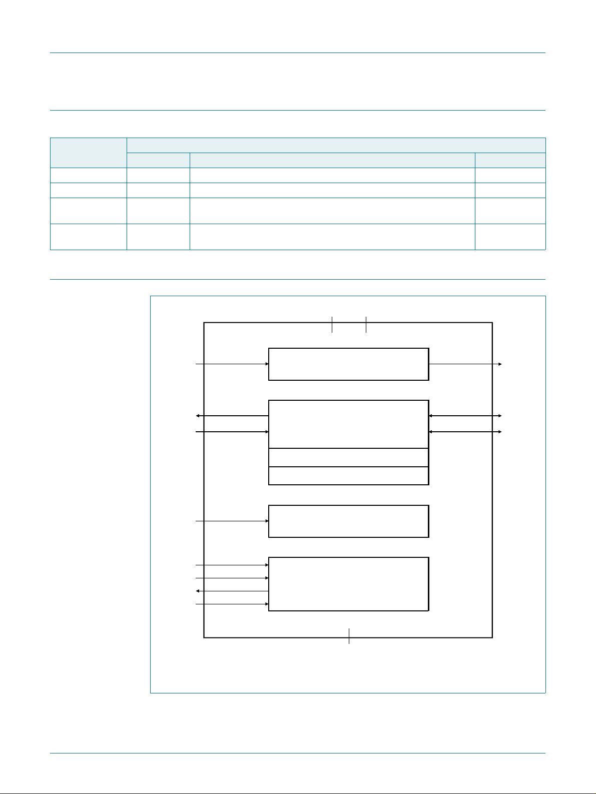
Advanced power management regulates the supply throughout the node and supports
local and remote wake-up functionality. I/O levels are automatically adjusted to the I/O
levels of the controller, allowing the TJA1145 to interface directly with 3.3 V to 5 V
microcontrollers. An SPI interface is provided for transceiver control and for retrieving
status information. Bus connections are truly floating when power is off.
The TJA1145 implements the CAN physical layer as defined in ISO 11898-2:2016 and
SAE J2284-1 to SAE J2284-4. This implementation enables reliable communication in the
CAN FD fast phase at data rates up to 2 Mbit/s.
These features make the TJA1145 the ideal choice for high-speed CAN networks
containing nodes that are always connected to the battery supply line but, in order to
minimize current consumption, are only active when required by the application.
2. Features and benefits
2.1 General
ISO 11898-2:2016 and SAE J2284-1 to SAE J2284-4 compliant
Timing guaranteed for data rates up to 2 Mbit/s
Autonomous bus biasing according to ISO 11898-2:2016
Optimized for in-vehicle high-speed CAN communication
No ‘false’ wake-ups due to CAN FD in TJA1145/FD variants
TJA1145
High-speed CAN transceiver for partial networking
Rev. 4 — 09 May 2018 Product data sheet
TJA1145 All information provided in this document is subject to legal disclaimers. © NXP Semiconductors N.V. 2018. All rights reserved.
Product data sheet Rev. 4 — 09 May 2018 2 of 57
NXP Semiconductors
TJA1145
High-speed CAN transceiver for partial networking
2.2 Designed for automotive applications
8 kV ElectroStatic Discharge (ESD) protection, according to the Human Body Model
(HBM) on the CAN bus pins
6 kV ESD protection, according to IEC 61000-4-2 on pins BAT and WAKE and on the
CAN bus pins
CAN bus pins short-circuit proof to 58 V
Battery and CAN bus pins protected against transients according to ISO 7637-3, test
pulses 1, 2a, 3a and 3b.
Suitable for use in 12 V and 24 V systems
Available in SO14 and leadless HVSON14 package (3 mm 4.5 mm) with improved
Automated Optical Inspection (AOI) capability
AEC-Q100 qualified
Dark green product (halogen free and Restriction of Hazardous Substances (RoHS)
compliant)
2.3 Advanced ECU power management system
Very low-current Standby and Sleep modes, with full wake-up capability
Entire node can be powered down via the inhibit output
Remote wake-up capability via standard CAN wake-up pattern or via
ISO 11898-2:2016 compliant selective wake-up frame detection
Local wake-up via the WAKE pin
Wake-up source recognition
Bit rates of 50 kbit/s, 100 kbit/s, 125 kbit/s, 250 kbit/s, 500 kbit/s and 1 Mbit/s
supported during selective wake-up'
Local and/or remote wake-up can be disabled to reduce current consumption
Transceiver disengages from the bus when the battery supply is removed
VIO input allows for direct interfacing with 3.3 V to 5 V microcontrollers
2.4 Protection and diagnosis
16-, 24- or 32-bit SPI for configuration, control and diagnosis
Transmit Data (TXD) dominant time-out function with diagnosis
Overtemperature warning and shut-down
Undervoltage detection and recovery on pins VCC, VIO and BAT
Cold start diagnosis (via bits PO and NMS)
Advanced system and transceiver interrupt handling
TJA1145 All information provided in this document is subject to legal disclaimers. © NXP Semiconductors N.V. 2018. All rights reserved.
Product data sheet Rev. 4 — 09 May 2018 3 of 57
NXP Semiconductors
TJA1145
High-speed CAN transceiver for partial networking
3. Quick reference data
Table 1. Quick reference data
Symbol Parameter Conditions Min Typ Max Unit
V
BAT
battery supply voltage 4.5 - 28 V
V
CC
supply voltage 4.5 - 5.5 V
V
IO
supply voltage on pin V
IO
2.85 - 5.5 V
V
th(det)poff
power-off detection threshold
voltage
V
BAT
falling 2.8 - 3 V
V
uvd(VCC)
undervoltage detection voltage
on pin VCC
4.5 - 4.75 V
V
uvd(VIO)
undervoltage detection voltage
on pin VIO
V
BAT
> 4.5 V 2.7 - 2.85 V
I
BAT
battery supply current Normal mode - 1 1.5 mA
Sleep mode; CAN Offline mode;
40 C < T
vj
<85C; V
BAT
= 7 V to 18 V
-4059A
Standby mode; CAN Offline mode;
40 C < T
vj
<85C; V
BAT
= 7 V to 18 V
-4468A
I
CC
supply current CAN Active mode; CAN recessive; V
TXD
=V
IO
-36mA
CAN Active mode; CAN dominant; V
TXD
= 0 V - 45 65 mA
Standby/Normal mode; CAN inactive;
40 C < T
vj
<85C
-4.78.5A
Sleep mode; CAN inactive; 40 C < T
vj
<85C- 3.87 A
I
IO
supply current on pin V
IO
Standby/Normal mode; 40 C < T
vj
<85C-7.111A
Sleep mode; 40 C < T
vj
<85C-58A
V
ESD
electrostatic discharge voltage IEC 61000-4-2 on pins CANH, CANL 6- +6kV
V
CANH
voltage on pin CANH 58 - +58 V
V
CANL
voltage on pin CANL 58 - +58 V
T
vj
virtual junction temperature 40 - +150 C
TJA1145 All information provided in this document is subject to legal disclaimers. © NXP Semiconductors N.V. 2018. All rights reserved.
Product data sheet Rev. 4 — 09 May 2018 4 of 57
NXP Semiconductors
TJA1145
High-speed CAN transceiver for partial networking
4. Ordering information
5. Block diagram
Table 2. Ordering information
Type number Package
Name Description Version
TJA1145T SO14 plastic small outline package; 14 leads; body width 3.9 mm SOT108-1
TJA1145T/FD SO14 plastic small outline package; 14 leads; body width 3.9 mm SOT108-1
TJA1145TK HVSON14 plastic thermal enhanced very thin small outline package; no leads;
14 terminals; body 3 4.5 0.85 mm
SOT1086-2
TJA1145TK/FD HVSON14 plastic thermal enhanced very thin small outline package; no leads;
14 terminals; body 3 4.5 0.85 mm
SOT1086-2
(1) TJA1145T/FD and TJA1145TK/FD only.
Fig 1. Block diagram
7-$
%$7
,1+
,1+
+6&$1
3$57,$/1(7:25.,1*
:$.(
:$.(83
6',
6&.
6&61
6'2
63,
DDD
&$1+
&$1/
7;'
5;'
*1'
9&&
9,2
&$1)'SDVVLYH
TJA1145 All information provided in this document is subject to legal disclaimers. © NXP Semiconductors N.V. 2018. All rights reserved.
Product data sheet Rev. 4 — 09 May 2018 5 of 57
NXP Semiconductors
TJA1145
High-speed CAN transceiver for partial networking
6. Pinning information
6.1 Pinning
6.2 Pin description
[1] HVSON14 package die supply ground is connected to both the GND pin and the exposed center pad. The
GND pin must be soldered to board ground. For enhanced thermal and electrical performance, it is
recommended that the exposed center pad also be soldered to board ground
Fig 2. Pin configuration diagram: SO14 Fig 3. Pin configuration diagram: HVSON14
Transparent top view
7-$7
7-$7)'
DDD
7;' 6&61
*1' &$1+
9&& &$1/
5;' 6',
9,2 %$7
6'2 :$.(
,1+ 6&.
WHUPLQDO
LQGH[DUHD
7-$7.
7-$7.)'
DDD
7;'
*1'
5;'
9,2
6'2
,1+
6&61
&$1+
&$1/
6',
%$7
:$.(
6&.
9&&
Table 3. Pin description
Symbol Pin Description
TXD 1 transmit data input
GND 2
[1]
ground
VCC 3 5 V CAN transceiver supply voltage
RXD 4 receive data output; reads out data from the bus lines
VIO 5 supply voltage for I/O level adaptor
SDO 6 SPI data output
INH 7 inhibit output for switching external voltage regulators
SCK 8 SPI clock input
WAKE 9 local wake-up input
BAT 10 battery supply voltage
SDI 11 SPI data input
CANL 12 LOW-level CAN bus line
CANH 13 HIGH-level CAN bus line
SCSN 14 SPI chip select input
剩余56页未读,继续阅读
zhimu
- 粉丝: 3
- 资源: 21
上传资源 快速赚钱
- 我的内容管理 收起
- 我的资源 快来上传第一个资源
- 我的收益 登录查看自己的收益
- 我的积分 登录查看自己的积分
- 我的C币 登录后查看C币余额
- 我的收藏
- 我的下载
- 下载帮助
会员权益专享
最新资源
- stc12c5a60s2 例程
- Android通过全局变量传递数据
- c++校园超市商品信息管理系统课程设计说明书(含源代码) (2).pdf
- 建筑供配电系统相关课件.pptx
- 企业管理规章制度及管理模式.doc
- vb打开摄像头.doc
- 云计算-可信计算中认证协议改进方案.pdf
- [详细完整版]单片机编程4.ppt
- c语言常用算法.pdf
- c++经典程序代码大全.pdf
- 单片机数字时钟资料.doc
- 11项目管理前沿1.0.pptx
- 基于ssm的“魅力”繁峙宣传网站的设计与实现论文.doc
- 智慧交通综合解决方案.pptx
- 建筑防潮设计-PowerPointPresentati.pptx
- SPC统计过程控制程序.pptx
资源上传下载、课程学习等过程中有任何疑问或建议,欢迎提出宝贵意见哦~我们会及时处理!
点击此处反馈
安全验证
文档复制为VIP权益,开通VIP直接复制
信息提交成功
评论1