CMOS, 330 MHz
Triple 10-Bit High Speed Video DAC
ADV7123
Rev. D
Information furnished by Analog Devices is believed to be accurate and reliable. However, no
responsibility is assumed by Analog Devices for its use, nor for any infringements of patents or other
rights of third parties that may result from its use. Specifications subject to change without notice. No
license is granted by implication or otherwise under any patent or patent rights of Analog Devices.
Trademarks and registered trademarks are the property of their respective owners.
One Technology Way, P.O. Box 9106, Norwood, MA 02062-9106, U.S.A.
Tel: 781.329.4700 www.analog.com
Fax: 781.461.3113 ©2010 Analog Devices, Inc. All rights reserved.
FEATURES
330 MSPS throughput rate
Triple 10-bit digital-to-analog converters (DACs)
SFDR
−70 dB at f
CLK
= 50 MHz; f
OUT
= 1 MHz
−53 dB at f
CLK
= 140 MHz; f
OUT
= 40 MHz
RS-343A-/RS-170-compatible output
Complementary outputs
DAC output current range: 2.0 mA to 26.5 mA
TTL-compatible inputs
Internal reference (1.235 V)
Single-supply 5 V/3.3 V operation
48-lead LQFP package
Low power dissipation (30 mW minimum @ 3 V)
Low power standby mode (6 mW typical @ 3 V)
Industrial temperature range (−40°C to +85°C)
Pb-free (lead-free) package
APPLICATIONS
Digital video systems (1600 × 1200 @ 100 Hz)
High resolution color graphics
Digital radio modulation
Image processing
Instrumentation
Video signal reconstruction
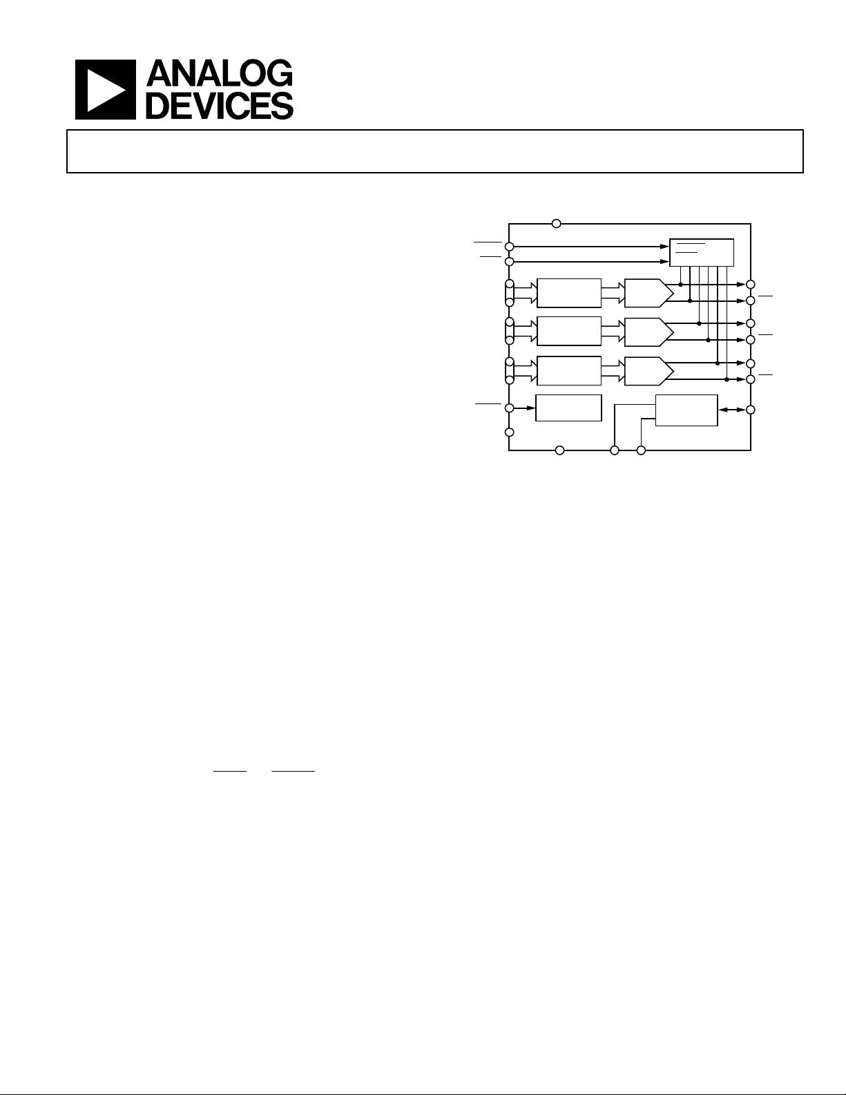
FUNCTIONAL BLOCK DIAGRAM
10
10
10
10
10
10
DATA
REGISTER
DAC
DAC
BLANK
SYNC
R9 TO R0
G9 TO G0
B9 TO B0
PSAVE
CLOCK
DAC
ADV7123
DATA
REGISTER
DATA
REGISTER
BLANK AND
SYNC LOGIC
POWER-DOWN
MODE
VOLTAGE
REFERENCE
CIRCUIT
IOR
IOR
IOG
IOG
IOB
V
REF
R
SET
V
AA
COMPGND
IOB
00215-001
Figure 1.
GENERAL DESCRIPTION
The ADV7123 (ADV®) is a triple high speed, digital-to-analog
converter on a single monolithic chip. It consists of three high
speed, 10-bit, video DACs with complementary outputs, a
standard TTL input interface, and a high impedance, analog
output current source.
The ADV7123 has three separate 10-bit-wide input ports. A
single 5 V/3.3 V power supply and clock are all that are required
to make the part functional. The ADV7123 has additional video
control signals, composite
SYNC
and
BLANK
.
The ADV7123 also has a power save mode.
The ADV7123 is fabricated in a 5 V CMOS process. Its
monolithic CMOS construction ensures greater functionality
with lower power dissipation. The ADV7123 is available in a
48-lead LQFP package.
PRODUCT HIGHLIGHTS
1. 330 MSPS throughput.
2. Guaranteed monotonic to 10 bits.
3. Compatible with a wide variety of high resolution color
graphics systems, including RS-343A and RS-170.
ADV is a registered trademark of Analog Devices, Inc.


剩余23页未读,继续阅读

GreatXXXX
- 粉丝: 4
- 资源: 1
 我的内容管理
收起
我的内容管理
收起
- 我的资源
快来上传第一个资源
 我的收益 登录查看自己的收益
 我的积分
登录查看自己的积分
我的积分
登录查看自己的积分
 我的C币
登录后查看C币余额
我的C币
登录后查看C币余额
 我的收藏
我的收藏  我的下载
我的下载  下载帮助
下载帮助

会员权益专享


最新资源
- 数据结构1800题含完整答案详解.doc
- 医疗企业薪酬系统设计与管理方案.pptx
- 界面与表面技术界面理论与表面技术要点PPT学习教案.pptx
- Java集合排序及java集合类详解(Collection、List、Map、Set)讲解.pdf
- 网页浏览器的开发 (2).pdf
- 路由器原理与设计讲稿6-交换网络.pptx
- 火电厂锅炉过热汽温控制系统设计.doc
- 企业识别CIS系统手册[收集].pdf
- 物业管理基础知识.pptx
- 第4章财务预测.pptx
- 《集成电路工艺设计及器件特性分析》——实验教学计算机仿真系.pptx
- 局域网内共享文件提示没有访问权限的问题借鉴.pdf
- 第5章网络营销策略.pptx
- 固井质量测井原理PPT教案.pptx
- 毕业实习总结6篇.doc
- UGNX建模基础篇草图模块PPT学习教案.pptx
资源上传下载、课程学习等过程中有任何疑问或建议,欢迎提出宝贵意见哦~我们会及时处理!
点击此处反馈


评论0