LPDDR4 Specification Revision B Item 1824.42B
Page 2 of 310
P R O P O S E D
Reference: Update history
1. The update portion from JESD209-4A is described below.
Table 00 - Modification from JESD209-4A
Note: Modification parts are marked by a RED side bar.
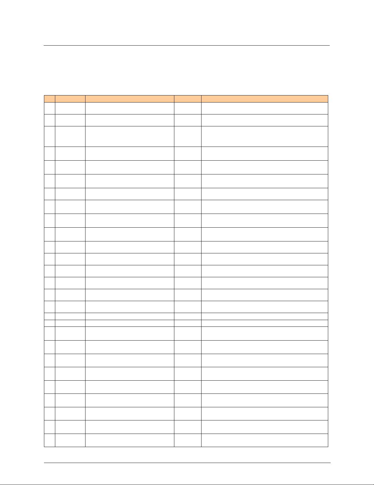
# Itme # Subject Page Reference
11831.95Scope 5
http://members.jedec.org/file_upload/filegallery/download-
document/index/document_id/51118
2 1831.95 Pad Order for single channel 7
http://members.jedec.org/file_upload/filegallery/download-
document/index/document_id/51118
31831.95
272-ball 15mm x 15mm 0.4mm pitch,
Quad-Channel POP FBGA (top view)
Using Variation VFFCDB for MO-273
8
http://members.jedec.org/file_upload/filegallery/download-
document/index/document_id/51118
41831.95
200-ball x32 Discrete Package, 0.80mm
x 0.65mm using MO-311
9-10
http://members.jedec.org/file_upload/filegallery/download-
document/index/document_id/51118
51831.95
203 ball Discrete Two-Channel FBGA
(top view) using MO-311
11
http://members.jedec.org/file_upload/filegallery/download-
document/index/document_id/51118
61831.95
432-ball x64 HDI Discrete Package,
0.50mm x 0.50mm (MO-313)
12
http://members.jedec.org/file_upload/filegallery/download-
document/index/document_id/51118
71831.95x64 Non HDI Discrete Package 13
http://members.jedec.org/file_upload/filegallery/download-
document/index/document_id/51118
81831.95
275 ball MCP Two-Channel FBGA (top
view) using MO-276
14
http://members.jedec.org/file_upload/filegallery/download-
document/index/document_id/51118
967.00A
254 ball eMMC MCP Two-Channel
FBGA (top view) using MO-276
15
JC63^20151221^67.00A^Mediatek_Micron_Samsung_SK_Hynix^
LPDDR4_2ch_254b_MCP.doc
10 67.00A
254 ball UFS MCP Two-Channel FBGA
(top view) using MO-276
16
JC63^20151221^67.00A^Mediatek_Micron_Samsung_SK_Hynix^
LPDDR4_2ch_254b_MCP.doc
11 1831.95 Pad Definition and Description 17
http://members.jedec.org/file_upload/filegallery/download-
document/index/document_id/51118
12 1831.95 Functional Description 18
http://members.jedec.org/file_upload/filegallery/download-
document/index/document_id/51118
13 1814.71A LPDDR4 SDRAM Addressing 19-20
http://members.jedec.org/file_upload/filegallery/download-
document/index/document_id/46507
14 1831.95 LPDDR4 SDRAM Addressing 19-22
http://members.jedec.org/file_upload/filegallery/download-
document/index/document_id/51118
15 1819.18C Simplified LPDDR4 State Diagram 23-25
http://members.jedec.org/file_upload/filegallery/download-
document/index/document_id/46552
16 1831.66 Mode Register Definition 30
http://members.jedec.org/file_upload/filegallery/download-
document/index/document_id/49876
17 1819.58A MR0 Register Information 31
https://vote.jedec.org/a_votingmachine/documents/RB15381-.pdf
18 1814.94A MR1 Register Information 32
https://vote.jedec.org/a_votingmachine/documents/RB15383-.pdf
19 1814.94A Burst Sequence 33
http://members.jedec.org/file_upload/filegallery/download-
document/index/document_id/46553
20 1831.95 MR3 Register Information 36
http://members.jedec.org/file_upload/filegallery/download-
document/index/document_id/51118
21 XXXX.XX MR4 Register Information 37
http://members.jedec.org/file_upload/filegallery/download-
document/index/document_id/44920
22 1831.95 MR8 Register Information 40
http://members.jedec.org/file_upload/filegallery/download-
document/index/document_id/51118
23 1819.05 MR11 Register Information 41
http://members.jedec.org/file_upload/filegallery/download-
document/index/document_id/48677
24 1819.06 MR12 Register Information 42-43
http://members.jedec.org/file_upload/filegallery/download-
document/index/document_id/46554
25 1831.95 MR16 Register Information 48
http://members.jedec.org/file_upload/filegallery/download-
document/index/document_id/51118
26 1831.95 MR17 Register Information 49
http://members.jedec.org/file_upload/filegallery/download-
document/index/document_id/51118
27 1831.66 MR30 Register Information 58
http://members.jedec.org/file_upload/filegallery/download-
document/index/document_id/49876


 我的内容管理
收起
我的内容管理
收起
 我的收益 登录查看自己的收益
 我的积分
登录查看自己的积分
我的积分
登录查看自己的积分
 我的C币
登录后查看C币余额
我的C币
登录后查看C币余额
 我的收藏
我的收藏  我的下载
我的下载  下载帮助
下载帮助 


评论0