没有合适的资源?快使用搜索试试~ 我知道了~
首页PCA 9546A I2C扩展芯片spec
PCA 9546A I2C扩展芯片spec
需积分: 50 23 下载量 174 浏览量
更新于2023-03-16
评论
收藏 2.24MB PDF 举报
PCA 9546A I2C扩展芯片spec,可以用于一组I2C控制输出4组I2C信号,硬件软件都可以参考的一篇资料
资源详情
资源评论
资源推荐
PCA9546A
Slaves A0, A1...AN
Slaves B0, B1...BN
Slaves C0, C1...CN
Slaves D0, D1...DN
I2C or SMBus
Master
(e.g. Processor)
SDA
SCL
SD0
SC0
Channel 0
Channel 1
Channel 2
Channel 3
RESET
SD1
SC1
SD2
SC2
SD3
SC3
V
CC
A1
A2
GND
A0
Copyright © 2016, Texas Instruments Incorporated
Product
Folder
Sample &
Buy
Technical
Documents
Tools &
Software
Support &
Community
An IMPORTANT NOTICE at the end of this data sheet addresses availability, warranty, changes, use in safety-critical applications,
intellectual property matters and other important disclaimers. PRODUCTION DATA.
PCA9546A
SCPS148G –OCTOBER 2005–REVISED MAY 2016
PCA9546A Low Voltage 4-Channel I
2
C and SMBus Switch with Reset Function
1
1 Features
1
• 1-of-4 Bidirectional Translating Switches
• I
2
C Bus and SMBus Compatible
• Active-Low Reset Input
• Three Address Pins, Allowing up to Eight
PCA9546A Devices on the I
2
C Bus
• Channel Selection Via I
2
C Bus, in Any
Combination
• Power-up With All Switch Channels Deselected
• Low R
ON
Switches
• Allows Voltage-Level Translation Between
1.8-V, 2.5-V, 3.3-V, and 5-V Buses
• No Glitch on Power-up
• Supports Hot Insertion
• Low Standby Current
• Operating Power-Supply Voltage Range of 2.3 V
to 5.5 V
• 5.5 V Tolerant Inputs
• 0 to 400-kHz Clock Frequency
• Latch-Up Performance Exceeds 100 mA Per
JESD 78
• ESD Protection Exceeds JESD 22
– 2000-V Human-Body Model (A114-A)
– 1000-V Charged-Device Model (C101)
(1) For all available packages, see the orderable addendum at
the end of the datasheet.
2 Applications
• Servers
• Routers (Telecom Switching Equipment)
• Factory Automation
• Products With I
2
C Slave Address Conflicts
(for example. Multiple, Identical Temp Sensors)
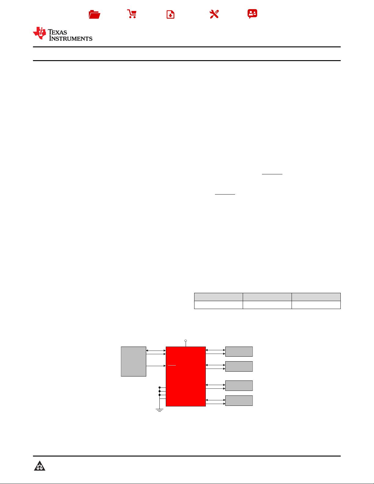
3 Description
The PCA9546A is a quad bidirectional translating
switch controlled via the I
2
C bus. The SCL/SDA
upstream pair fans out to four downstream pairs, or
channels. Any individual SCn/SDn channel or
combination of channels can be selected, determined
by the contents of the programmable control register.
An active-low reset (RESET) input allows the
PCA9546A to recover from a situation in which one of
the downstream I
2
C buses is stuck in a low state.
Pulling RESET low resets the I
2
C state machine and
causes all the channels to be deselected, as does the
internal power-on reset function.
The pass gates of the switches are constructed such
that the V
CC
pin can be used to limit the maximum
high voltage, which will be passed by the PCA9546A.
This allows the use of different bus voltages on each
pair, so that 1.8-V, 2.5-V, or 3.3-V parts can
communicate with 5-V parts without any additional
protection. External pull-up resistors pull the bus up
to the desired voltage level for each channel. All I/O
pins are 5.5-V tolerant.
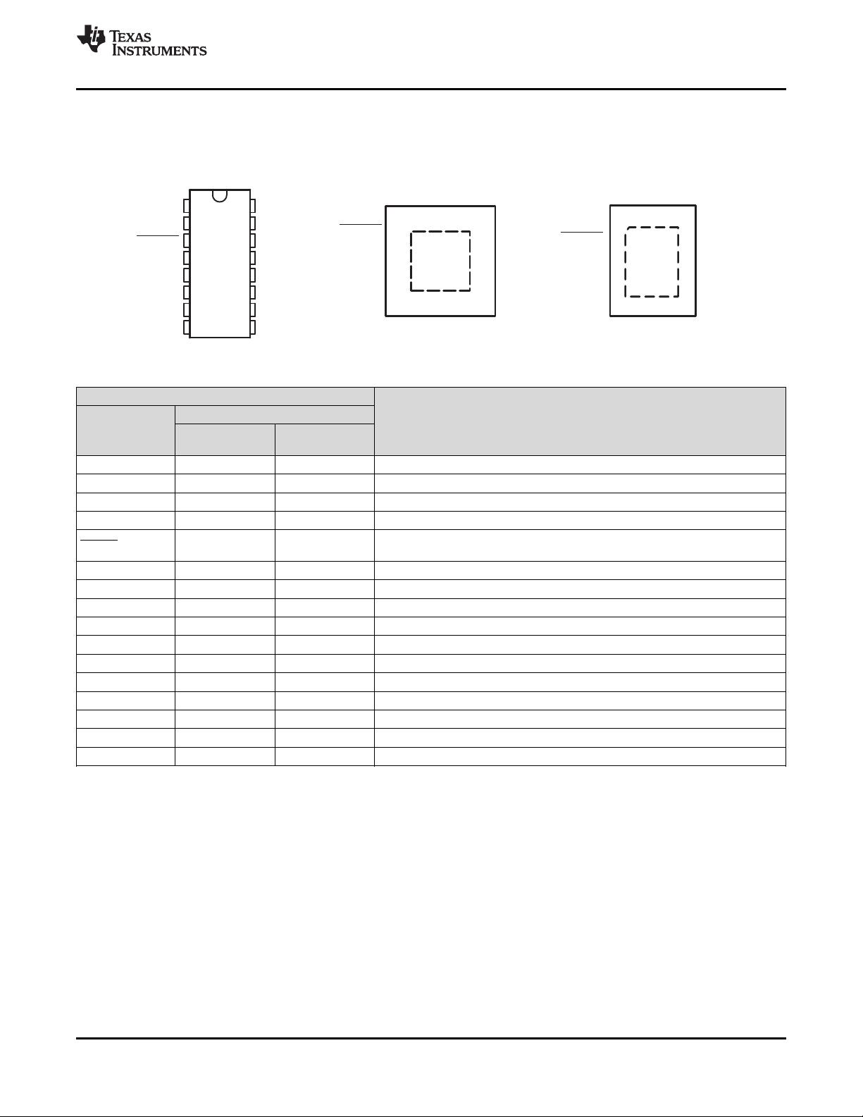
Device Information
(1)
PART NUMBER PACKAGE BODY SIZE (NOM)
PCA9546A TSSOP (16) 5.00 mm x 4.40 mm
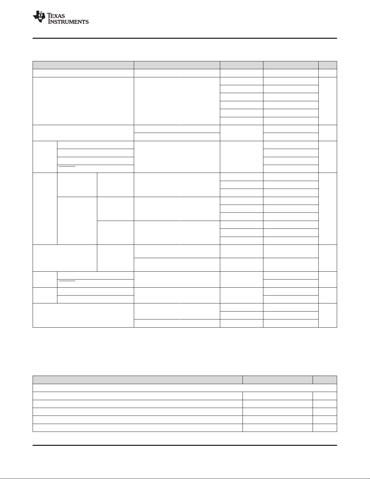
Simplified Application Diagram
2
PCA9546A
SCPS148G –OCTOBER 2005–REVISED MAY 2016
www.ti.com
Product Folder Links: PCA9546A
Submit Documentation Feedback Copyright © 2005–2016, Texas Instruments Incorporated
Table of Contents
1 Features.................................................................. 1
2 Applications ........................................................... 1
3 Description ............................................................. 1
4 Revision History..................................................... 2
5 Pin Configuration and Functions......................... 3
6 Specifications......................................................... 4
6.1 Absolute Maximum Ratings ..................................... 4
6.2 ESD Ratings ............................................................ 4
6.3 Recommended Operating Conditions ...................... 4
6.4 Electrical Characteristics........................................... 5
6.5 I
2
C Interface Timing Requirements.......................... 5
6.6 Interrupt and Reset Timing Requirements................ 7
6.7 Switching Characteristics.......................................... 7
7 Parameter Measurement Information .................. 8
8 Detailed Description............................................ 10
8.1 Overview ................................................................. 10
8.2 Functional Block Diagram ....................................... 10
8.3 Feature Description................................................. 11
8.4 Device Functional Modes........................................ 11
8.5 Programming........................................................... 11
8.6 Control Register ...................................................... 14
9 Application and Implementation ........................ 15
9.1 Application Information............................................ 15
9.2 Typical Application .................................................. 15
10 Power Supply Recommendations ..................... 19
10.1 Power-On Reset Errata......................................... 19
11 Layout................................................................... 19
11.1 Layout Guidelines ................................................. 19
11.2 Layout Example .................................................... 20
12 Device and Documentation Support ................. 20
12.1 Electrostatic Discharge Caution............................ 20
12.2 Glossary................................................................ 20
13 Mechanical, Packaging, and Orderable
Information ........................................................... 20
4 Revision History
NOTE: Page numbers for previous revisions may differ from page numbers in the current version.
Changes from Revision F (April 2014) to Revision G Page
• Revised pack material addendum; pin 1 quadrant .............................................................................................................. 20
Changes from Revision E (January 2008) to Revision F Page
• Added RESET Errata section............................................................................................................................................... 11
• Added Power-On Reset Errata section. ............................................................................................................................... 19
D, DGV, DW, OR PW PACKAGE
(TOP VIEW)
1
2
3
4
5
6
7
8
16
15
14
13
12
11
10
9
A0
A1
RESET
SD0
SC0
SD1
SC1
GND
V
CC
SDA
SCL
A2
SC3
SD3
SC2
SD2
RGY PACKAGE
(TOP VIEW)
2
15
SDAA1
3
14
SCL
RESET
4
13
A2SD0
5
12
SC3SC0
6
11
SD3SD1
7
10
SC2SC1
1
8
A0
GND
16
9
SD2
V
CC
RGV PACKAGE
(TOP VIEW)
8
SC2
13
SDA
16
5
A1
SC1
6
15
A0
GND
V
CC
7
14
SD2
1 12
SCL
RESET
2 11
A2SD0
10
SC3
3
SC0
4
9
SD3SD1
3
PCA9546A
www.ti.com
SCPS148G –OCTOBER 2005–REVISED MAY 2016
Product Folder Links: PCA9546A
Submit Documentation FeedbackCopyright © 2005–2016, Texas Instruments Incorporated
(1) V
DPUX
is the pull-up reference voltage for the associated data line. V
DPUM
is the master I
2
C reference voltage while V
DPU0
- V
DPU3
are
the slave channel reference voltages.
5 Pin Configuration and Functions
Pin Functions
PIN
DESCRIPTION
NAME
NO.
D, DGV, DW,
PW, AND RGY
RGV
A0 1 15 Address input 0. Connect directly to V
CC
or ground
A1 2 16 Address input 1. Connect directly to V
CC
or ground
A2 13 11 Address input 2. Connect directly to V
CC
or ground
GND 8 6 Ground
RESET 3 1
Active low reset input. Connect to V
DPUM
(1)
through a pull-up resistor, if not
used.
SD0 4 2 Serial data 0. Connect to V
DPU0
(1)
through a pull-up resistor
SC0 5 3 Serial clock 0. Connect to V
DPU0
(1)
through a pull-up resistor
SD1 6 4 Serial data 1. Connect to V
DPU1
(1)
through a pull-up resistor
SC1 7 5 Serial clock 1. Connect to V
DPU1
(1)
through a pull-up resistor
SD2 9 7 Serial data 2. Connect to V
DPU2
(1)
through a pull-up resistor
SC2 10 8 Serial clock 2. Connect to V
DPU2
(1)
through a pull-up resistor
SD3 11 9 Serial data 3. Connect to V
DPU3
(1)
through a pull-up resistor.
SC3 12 10 Serial clock 3. Connect to V
DPU3
(1)
through a pull-up resistor
SCL 14 12 Serial clock line. Connect to V
DPUM
(1)
through a pull-up resistor
SDA 15 13 Serial data line. Connect to V
DPUM
(1)
through a pull-up resistor
V
CC
16 14 Supply power
4
PCA9546A
SCPS148G –OCTOBER 2005–REVISED MAY 2016
www.ti.com
Product Folder Links: PCA9546A
Submit Documentation Feedback Copyright © 2005–2016, Texas Instruments Incorporated
(1) Stresses beyond those listed under Absolute Maximum Ratings may cause permanent damage to the device. These are stress ratings
only, which do not imply functional operation of the device at these or any other conditions beyond those indicated under Recommended
Operating Conditions. Exposure to absolute-maximum-rated conditions for extended periods may affect device reliability.
(2) The input negative-voltage and output voltage ratings may be exceeded if the input and output current ratings are observed.
(3) The package thermal impedance is calculated in accordance with JESD 51-7.
6 Specifications
6.1 Absolute Maximum Ratings
(1)
over operating free-air temperature range (unless otherwise noted)
MIN MAX UNIT
V
CC
Supply voltage –0.5 7 V
V
I
Input voltage
(2)
–0.5 7 V
I
I
Input current ±20 mA
I
O
Output current ±25 mA
Continuous current through V
CC
±100 mA
Continuous current through GND ±100 mA
θ
JA
Package thermal impedance
(3)
D package 73
°C/W
DGV package 120
DW package 57
PW package 108
RGV package 51.38
RGY package 50
P
tot
Total power dissipation 400 mW
T
A
Operating free-air temperature –40 85 °C
T
stg
Storage temperature –65 150
(1) JEDEC document JEP155 states that 500-V HBM allows safe manufacturing with a standard ESD control process.
(2) JEDEC document JEP157 states that 250-V CDM allows safe manufacturing with a standard ESD control process.
6.2 ESD Ratings
VALUE UNIT
V
(ESD)
Electrostatic discharge
Human-body model (HBM), per ANSI/ESDA/JEDEC JS-001
(1)
±2000
V
Charged-device model (CDM), per JEDEC specification JESD22-
C101
(2)
±1000
(1) All unused inputs of the device must be held at V
CC
or GND to ensure proper device operation. Refer to the TI application report,
Implications of Slow or Floating CMOS Inputs, SCBA004.
6.3 Recommended Operating Conditions
(1)
MIN MAX UNIT
V
CC
Supply voltage 2.3 5.5 V
V
IH
High-level input voltage
SCL, SDA 0.7 × V
CC
6
V
A2–A0, RESET 0.7 × V
CC
V
CC
+ 0.5
V
IL
Low-level input voltage
SCL, SDA –0.5 0.3 × V
CC
V
A2–A0, RESET –0.5 0.3 × V
CC
T
A
Operating free-air temperature –40 85 °C
5
PCA9546A
www.ti.com
SCPS148G –OCTOBER 2005–REVISED MAY 2016
Product Folder Links: PCA9546A
Submit Documentation FeedbackCopyright © 2005–2016, Texas Instruments Incorporated
(1) All typical values are at nominal supply voltage (2.5-V, 3.3-V, or 5-V V
CC
), T
A
= 25°C.
(2) The power-on reset circuit resets the I
2
C bus logic with V
CC
< V
POR
. V
CC
must be lowered to 0.2 V to reset the device.
(3) C
io(ON)
depends on internal capacitance and external capacitance added to the SCn lines when channels(s) are ON.
6.4 Electrical Characteristics
over recommended operating free-air temperature range (unless otherwise noted)
PARAMETER TEST CONDITIONS V
CC
MIN TYP
(1)
MAX UNIT
V
POR
Power-on reset voltage
(2)
No load, V
I
= V
CC
or GND V
POR
1.6 2.1 V
V
pass
Switch output voltage V
SWin
= V
CC
, I
SWout
= –100 μA
5 V 3.6
V
4.5 V to 5.5 V 2.6 4.5
3.3 V 1.9
3 V to 3.6 V 1.6 2.8
2.5 V 1.5
2.3 V to 2.7 V 1.1 2
I
OL
SCL, SDA
V
OL
= 0.4 V
2.3 V to 5.5 V
3 7
mA
V
OL
= 0.6 V 6 10
I
I
SCL, SDA
V
I
= V
CC
or GND 2.3 V to 5.5 V
±1
μA
SC3–SC0, SD3–SD0 ±1
A2–A0 ±1
RESET ±1
I
CC
Operating mode f
SCL
= 100 kHz V
I
= V
CC
or GND, I
O
= 0
5.5 V 3 12
μA
3.6 V 3 11
2.7 V 3 10
Standby mode
Low inputs V
I
= GND, I
O
= 0
5.5 V 0.3 1
3.6 V 0.1 1
2.7 V 0.1 1
High inputs V
I
= V
CC
, I
O
= 0
5.5 V 0.3 1
3.6 V 0.1 1
2.7 V 0.1 1
ΔI
CC
Supply-current
change
SCL, SDA
SCL or SDA input at 0.6 V,
Other inputs at V
CC
or GND
8 15
μA
SCL or SDA input at V
CC
– 0.6 V,
Other inputs at V
CC
or GND
2.3 V to 5.5 V 8 15
C
i
A2–A0
V
I
= V
CC
or GND 2.3 V to 5.5 V
4.5 6
pF
RESET 4.5 5.5
C
io(OFF)
(3)
SCL, SDA
V
I
= V
CC
or GND, Switch OFF 2.3 V to 5.5 V
15 19
pF
SC3–SC0, SD3–SD0 6 8
R
ON
Switch on-state resistance
V
O
= 0.4 V, I
O
= 15 mA
4.5 V to 5.5 V 4 9 16
Ω3 V to 3.6 V 5 11 20
V
O
= 0.4 V, I
O
= 10 mA 2.3 V to 2.7 V 7 16 45
6.5 I
2
C Interface Timing Requirements
over recommended operating free-air temperature range (unless otherwise noted) (see Figure 1)
MIN MAX UNIT
I
2
C BUS—STANDARD MODE
f
scl
I
2
C clock frequency 0 100 kHz
t
sch
I
2
C clock high time 4 µs
t
scl
I
2
C clock low time 4.7 µs
t
sp
I
2
C spike time 50 ns
t
sds
I
2
C serial-data setup time 250 ns
剩余39页未读,继续阅读
txjily
- 粉丝: 19
- 资源: 4
上传资源 快速赚钱
- 我的内容管理 收起
- 我的资源 快来上传第一个资源
- 我的收益 登录查看自己的收益
- 我的积分 登录查看自己的积分
- 我的C币 登录后查看C币余额
- 我的收藏
- 我的下载
- 下载帮助
会员权益专享
最新资源
- stc12c5a60s2 例程
- Android通过全局变量传递数据
- c++校园超市商品信息管理系统课程设计说明书(含源代码) (2).pdf
- 建筑供配电系统相关课件.pptx
- 企业管理规章制度及管理模式.doc
- vb打开摄像头.doc
- 云计算-可信计算中认证协议改进方案.pdf
- [详细完整版]单片机编程4.ppt
- c语言常用算法.pdf
- c++经典程序代码大全.pdf
- 单片机数字时钟资料.doc
- 11项目管理前沿1.0.pptx
- 基于ssm的“魅力”繁峙宣传网站的设计与实现论文.doc
- 智慧交通综合解决方案.pptx
- 建筑防潮设计-PowerPointPresentati.pptx
- SPC统计过程控制程序.pptx
资源上传下载、课程学习等过程中有任何疑问或建议,欢迎提出宝贵意见哦~我们会及时处理!
点击此处反馈
安全验证
文档复制为VIP权益,开通VIP直接复制
信息提交成功
评论0