没有合适的资源?快使用搜索试试~ 我知道了~
首页PMSM/BLDC驱动器开发智能预驱芯片TMC6200带有SPI通讯
TMC6200 是一款 PMSM 和 BLDC 伺服电机大功率预驱芯片,使用外部 6 个 MOSFETs 和 2 个或 3 个检测电阻。集成了 PMSM 驱动系统的全压部分 12V,24V 或 48V,带有可编程的在线电流检测放大器,可以驱动高达数千瓦的宽范围电机, 软件控制的驱动强度允许在系统内部高速优化。可编程的安全特性如短路检测, 超温阀值,以及用于诊断的 SPI 接口,可实现全面诊断和高可靠设计,最大限度 减少外部器件数量,增强系统保护和诊断能力
资源详情
资源评论
资源推荐

www.trinamic.com.cn
gao@trinamic.cn T:138-1261-7052
TMC6200
简介
TMC6200
是一款
PMSM
和
BLDC
伺服电 机 大 功 率 预驱芯片, 使 用 外 部
6
个
MOSFETs
和
2
个或
3
个检测电阻。集成了
PMSM
驱动系统的全压部分
12V
,
24V
或
48V
,带有可编程的在线电流检测放大器,可以驱动高达数千瓦的宽范围电机,
软件控制的驱动强度允许在系统内部高速优化。可编程的安全特性如短路检测,
超温阀值,以及用于诊断的
SPI
接口,可实现全面诊断和高可靠设计,最大限度
减少外部器件数量,增强系统保护和诊断能力
TMC6200-TA TMC6200-BOB
性能参数
- 外扩 MOSFETs 三相电机最大电流可达 100A 预驱,8-60V DC
- 可编程门驱电流 0.5A/1A/1.5A
- 通过 SPI 具备齐全的保护和诊断功能
- 具有可编程增益的浮动感测放大器(5,10,20)
- 带有 1Ω (LS) / 1.3Ω (HS) 门驱关闭安全延迟电阻
- SPI 或独立工作两种模式,100%循环电荷泵
- 可编程的短路,过载电流限制和重启。齐全的保护和诊断功能
- 9x9mm2 TQFP48 封装
系统框图
市场应用
PMSM/BLDC FOC 驱动
工厂自动化
实验室自动化
机器人/CNC 设备
纺织设备,智能家居
监控设备,打印机,泵

POWER DRIVER FOR STEPPER MOTORS INTEGRATED CIRCUITS
TRINAMIC Motion Control GmbH & Co. KG
Hamburg, Germany
TMC6200 DATASHEET
FEATURES AND BENEFITS
3-phase motors up to 100A coil current (external MOSFETs)
Voltage Range 8 … 60V DC
Gate Drive Programmable 0.5A / 1A / 1.5A
Full Protection and Diagnostics via SPI interface
3 Floating Sense Amplifiers with programmable gain (5, 10, 20)
Gate Off Drive with 1Ω (LS) / 1.3Ω (HS) safe hold off resistance
SPI & Stand-Alone operation
Charge Pump for 100% Duty Cycle operation
Optional BBM break-before-make logic for single line control
Programmable Short and Overload current threshold and retry
Programmable Control Interface with 3 line or 6 line drive
Full Protection & Diagnostics
Compact Size 9x9mm
2
TQFP48 package
Double Pin Distance for safe operation at high voltage
APPLICATIONS
PMSM FOC drives and BLDC motors
Industrial Drives
Factory Automation
Lab Automation
Robotics
CNC machines
Textile Machines
Pumps
Surveillance Cameras
Home Automation
Printers
DESCRIPTION
The TMC6200 is a high-power gate-driver
for PMSM servo or BLDC motors. Using
six external MOSFETs and two or three
sense resistors, it integrates the full high
voltage part of a PMSM drive system for
12V, 24V or 48V, including in-line current
sense amplifiers with programmable
amplification. It can drive a wide range
of motors from Watt to Kilowatt.
Software controlled drive strength allows
in-system EME optimization. Programm-
able safety features like short detection
and overtemperature thresholds together
with an SPI interface for diagnostics
allow robust and reliable designs. With
the TMC6200, a minimum number of
external components is required to build
a rugged drive with full protection and
diagnostics.
Universal high voltage BLDC/PMSM/Servo MOSFET 3-halfbridge gate-driver with in line motor current
sensing. External MOSFETs for up to 100A motor current.
BLOCK DIAGRAM
Driver
Logic
SPI / Pin setting
ENABLE
BHx
BLx
VCC_IO
Charge
Pump
VM
Power on
reset
5V / 12V
Regulator
RC
Oscillator
Current
Measurement
FAULT
+V
M
HS
LS
BLDC Motor
N
S
Short to GND, Short to VS
Undervoltage
Overtemperature
Diagnostics &
Error Feedback
Diagn. Comp.
CURU, V, W
GNDA
GNDP
µC or µC+
TMC4671
BUS / IO
LS-Drive
LS-Drive
HS-Drive
LS-Drive
LS-Drive
LS-Drive
RSW
RSU
TMC6200
Power
BM
CP
RS
RS
RS
RSV

TMC6200 DATASHEET (Rev. 1.03 / 2019-FEB-13) 2
www.trinamic.com
APPLICATION EXAMPLES: PMSM AND BLDC MOTORS
The TMC6200 scores with integration of the complete high-voltage part for FOC controlled PMSM drivers. On
the control side, it mates with sophisticated FOC TMC467x and TMC867x family controller chips, or with any
microcontroller. Its versatile interface matches simple BLDC drives with minimum requirements on the µC
PWM, as well as advanced PMSM control algorithms. The small form factor and easy-to-use package of the
TMC6200 keeps costs down and allows for miniaturized layouts. Extensive support at the chip, board, and
software levels enables rapid design cycles and fast time-to-market with competitive products. High
integration and reliability deliver cost savings in related systems such as power supplies and cooling.
CPU
TMC6200
High-Level
Interface
Gate CTRL
MINIATURIZED CPU BASED DESIGN FOR BLDC OR PMSM
HIGH PERFORMANCE FOC SERVO DESIGN FOR PMSM
M
Encoder
/ Hall
DIAG
SPI
(optional)
ADC
PWM
Current Sense
TMC6200
Gate CTRL
M
Encoder
/ Hall
SPI
Current
Sense
CPU
TMC467x
ADC
PWM
SPI
High-Level
Interface
ORDER CODES
Order code
Description
Size [mm
2
]
TMC6200-TA
Three phase gate-driver for external MOSFETs; TQFP48
9 x 9
TMC6200-TA-T
-T denotes tape on reel packed devices
TMC6200-EVAL
Evaluation board for TMC6200.
85 x 80
LANDUNGSBRÜCKE
Baseboard for TMC6200-EVAL and further evaluation boards.
85 x 55
ESELSBRÜCKE
Connector board for plug-in evaluation board system.
61 x 38
A CPU with internal BLDC or sine wave PWM
unit drives the gate control lines based on
encoder or hall sensor feedback. The current
sensor outputs become sampled by the µC
integrated ADC. Use of SPI is not required,
unless more sophisticated diagnostics is
desired.
When using one of the TRINAMIC FOC
controllers, the CPU is completely offloaded
from time-intensive regulation loop tasks,
and software design shrinks to initialization
and target parameter setting. The TMC6200
optimally complements a TMC467x family
controller.
The TMC6200-EVAL is part of TRINAMICs
universal evaluation board system which
provides a convenient handling of the
hardware as well as a user-friendly
software tool for evaluation. The
TMC6200 evaluation board system
consists of three parts:
LANDUNGSBRÜCKE (base board),
ESELSBRÜCKE (connector board including
several test points), and TMC6200-EVAL,
plus a TMC4671-EVAL FOC controller.

TMC6200 DATASHEET (Rev. 1.03 / 2019-FEB-13) 3
www.trinamic.com
Table of Contents
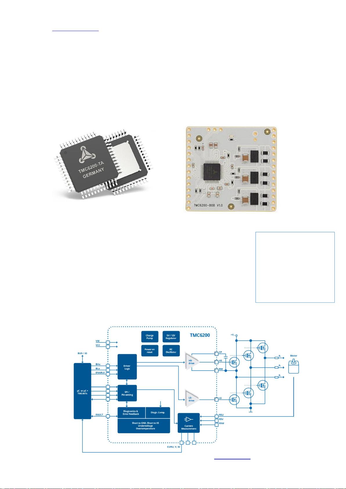
1 PRINCIPLES OF OPERATION ......................... 4
1.1 CONTROL INTERFACES ..................................... 6
2 PIN ASSIGNMENTS ........................................... 7
2.1 PACKAGE OUTLINE .......................................... 7
2.2 SIGNAL DESCRIPTIONS ................................... 7
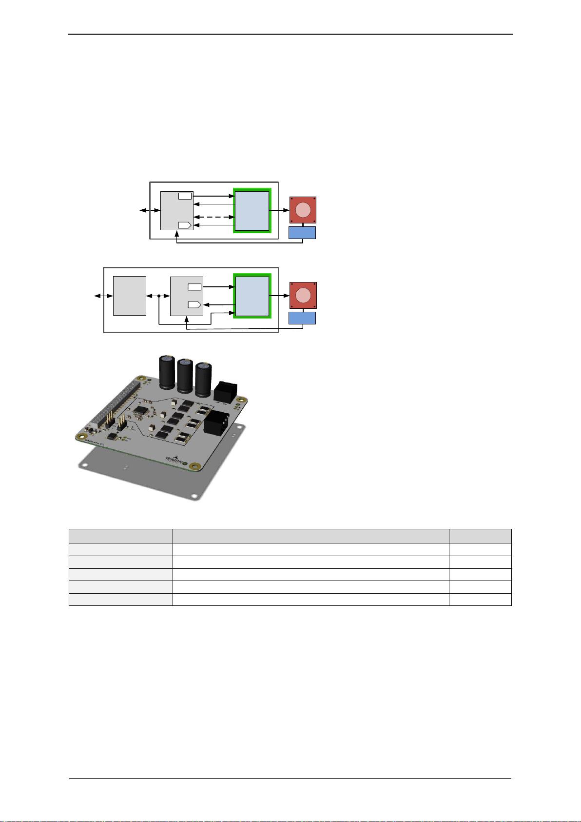
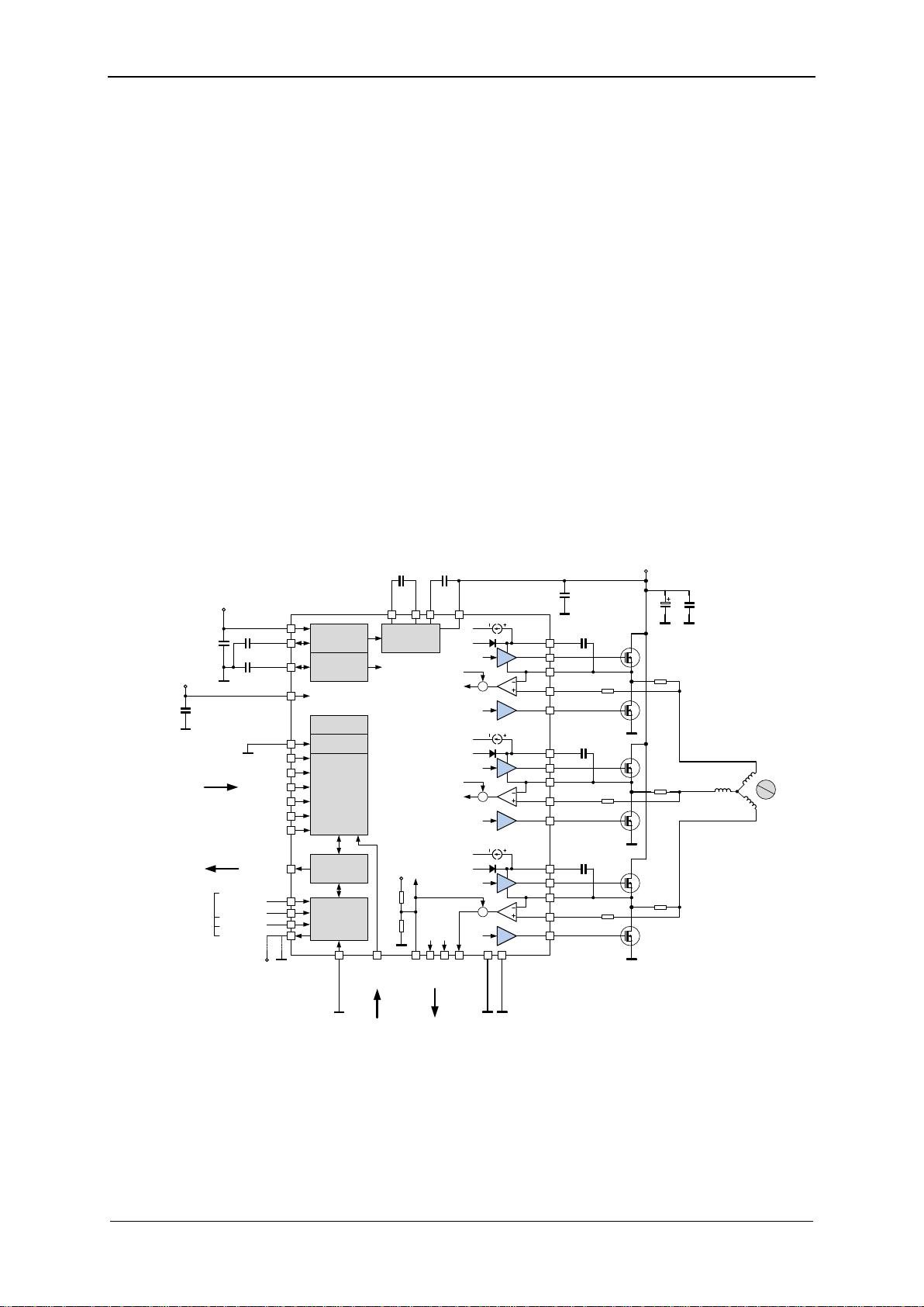
3 SAMPLE CIRCUITS .......................................... 10
3.1 STANDARD APPLICATION CIRCUIT ................ 10
3.2 EXTERNAL GATE VOLTAGE REGULATOR .......... 11
3.3 ZERO STANDBY CURRENT .............................. 12
3.4 MOSFETS AND SLOPE CONTROL .................. 13
3.5 TUNING THE MOSFET BRIDGE ..................... 15
4 SPI INTERFACE ................................................ 18
4.1 SPI DATAGRAM STRUCTURE ......................... 18
4.2 SPI SIGNALS ................................................ 19
4.3 TIMING ......................................................... 20
5 REGISTER MAPPING ....................................... 21
5.1 GENERAL CONFIGURATION REGISTERS .......... 22
6 CURRENT SENSE AMPLIFIERS ..................... 27
6.1 SETTLING TIME ............................................. 27
6.2 CURRENT AMPLIFIER OFFSET ........................ 28
6.3 CHOICE OF SENSE RESISTORS ....................... 31
7 DIAGNOSTICS AND PROTECTION ............. 32
7.1 TEMPERATURE SENSORS ................................ 32
7.2 SHORT PROTECTION ...................................... 32
8 EXTERNAL RESET ............................................. 34
9 CLOCK OSCILLATOR AND INPUT ............... 34
9.1 USING THE INTERNAL CLOCK ........................ 34
9.2 USING AN EXTERNAL CLOCK ......................... 34
10 ABSOLUTE MAXIMUM RATINGS ............ 35
11 ELECTRICAL CHARACTERISTICS ............ 35
11.1 OPERATIONAL RANGE ................................... 35
11.2 DC AND TIMING CHARACTERISTICS .............. 36
11.3 THERMAL CHARACTERISTICS.......................... 40
12 LAYOUT CONSIDERATIONS..................... 41
12.1 EXPOSED DIE PAD ........................................ 41
12.2 WIRING GND .............................................. 41
12.3 WIRING BRIDGE SUPPLY .............................. 41
12.4 SUPPLY FILTERING ........................................ 41
12.5 LAYOUT EXAMPLE ......................................... 42
13 PACKAGE MECHANICAL DATA ................ 44
13.1 DIMENSIONAL DRAWINGS TQFP48-EP ....... 44
13.2 PACKAGE CODES ........................................... 45
14 DISCLAIMER ................................................. 46
15 ESD SENSITIVE DEVICE............................ 46
16 TABLE OF FIGURES .................................... 47
17 REVISION HISTORY ................................... 47

TMC6200 DATASHEET (Rev. 1.03 / 2019-FEB-13) 4
www.trinamic.com
1 Principles of Operation
The TMC6200 is a MOSFET gate driver for three phase PMSM and BLDC motors. Ideally suited for
applications in the range of 12V to 48V, it supports motor power ratings from 1 Watt to 1kW. It
complements with TRINAMICs TMC467x & TMC867x families of three phase motor controller ICs.
Internal break-before-make timing is provided for the ease-of-use in combination with simple
microcontrollers for PWM generation. Integrated current sense amplifiers eliminate costly sense
amplifiers required for FOC controllers, while bringing the benefit of in-line current sensing. A
complete set of protection and diagnostic functions makes the power stage more rugged than a
discrete setup.
THE TMC6200 OFFERS TWO BASIC MODES OF OPERATION:
MODE 1: Stand-alone driver with pin configuration
Enable this mode by tying low pin SPE. The interface pins allow a number of different settings for
BBM generation and sense amplifier amplification control.
MODE 2: SPI controlled
This mode allows detailed control over the protection, diagnostic and control features, e.g. for tuning
overcurrent detection. Enable this mode by tying high pin SPE.
VCC_IO
TMC6200
Configuration
interface
CSN / IDRV0
SCK / IDRV1
SDO / SINGLE
SDI / AMPLx10
Diagnostics
(Short circuit,
Temperature)
5V Regulator
Charge Pump
22n
100V
100n
16V
FAULT
+V
M
5VOUT
VSA
2.2µ
+V
IO
DRV_EN
GNDA
DIE PAD
3.3V or 5V
I/O voltage
100n
100n
3 Phase
Motor
Break before
Make logic
100n
C
E
IU IV
CURV
CURU
CURW
Current Sense
SPE
Enable
B.Dwersteg, ©
TRINAMIC 2014
LS
USENSE
LSU
HSU
U
HS
CU
C
B
+V
M
CPI
CPO
VCP
VS
Gate Voltage
Regulator
12VOUT
4.7µ
470n
pd
pd
Sense Amplification 0: 5, 1: 10
0: xH/xL individual gate control
1: xH=Polarity, xL=Enable control
WL
WH
VL
VH
UL
UH
pd
pd
pd
pd
pd
N
S
RS
R
P
12VOUT
I
T
VCP
VOFS
LS
VSENSE
LSV
HSV
V
HS
CV
C
B
RS
R
P
12VOUT
VCP
LS
WSENSE
LSW
HSW
W
HS
CW
C
B
RS
R
P
12VOUT
VCP
I
T
I
T
IV
+
VOFS
IW
+
5VOUT
VOFS
24MHz Oscillator
OTP memory
CLK_IN
+
500k
250k
VOFS
Chopper Control
dual line LS+HS,
or single line
(HS=polarity, LS=enable)
+V
IO
01
Diagnostic Output
Driver Strength [IDRV1 IDRV0]:
00: 0.5A 01: 0.5/1A, 10: 1A, 11: 1.5A
Figure 1.1 Standalone application using differential sensing
剩余47页未读,继续阅读


安全验证
文档复制为VIP权益,开通VIP直接复制

评论0