没有合适的资源?快使用搜索试试~ 我知道了~
首页MT7621_ProgrammingGuide_Preliminary_Platform_decrypted.pdf
MT7621_ProgrammingGuide_Preliminary_Platform_decrypted.pdf
需积分: 49 914 浏览量
更新于2023-03-16
评论 1
收藏 8.61MB PDF 举报
mtk 7621开发编程指导,MT7621_ProgrammingGuide_Preliminary_Platform_decrypted.pdf
资源详情
资源评论
资源推荐

loginid=fan.yang@z-linkelec.com,time=2014-12-01 17:05:26,ip=183.37.105.173,doctitle=MT7621_ProgrammingGuide_Preliminary_Platform.pdf,company=Z-Link Limited 香港瑞聯電子_RLT
MT7621
PROGRAMMING
GUIDE
MEDIATEK CONFIDENTIAL

loginid=fan.yang@z-linkelec.com,time=2014-12-01 17:05:26,ip=183.37.105.173,doctitle=MT7621_ProgrammingGuide_Preliminary_Platform.pdf,company=Z-Link Limited 香港瑞聯電子_RLT
PGMT7621_V.1.0_130607 Page 2 of 349
MT7621 PROGRAMMING GUIDE
MT7621 Overview
The MT7621 SoC includes a high performance 880 MHz MIPS1004Kc CPU core and high speed
USB3.0/PCIe/SDXC interfaces, which is designed to enable a multitude of high performance, cost-effective IEEE
802.11n/ac applications with a MediaTek (Ralink) WiFi client card.
Functional Block Diagram
MIPS 1004Kc
32/32 KB I/D-
Cache per Core
(880 MHz)
OCP Bridge
OCP_IF
Arbiter
DRAM
Controller
RBUS
SPI
NFI
PBUS
GDMA/
HSDMA
RJ45 x5
Switch
(5GE)
5-Port EPHY
RGMII
TMII/MII x1
PCIe 1.1
PHY
USB 3.0/2.0
PHY
Host
PCIe x 3
UARTLx3
GPIO
PCM x4
I2S
I2C
I2S
PBUS
INTC
I2C
GPIO
/LED
SPI
NAND
UART
To CPU
interrupts
16-Bit DDR2/DDR3
EJTAG
Crypto
Engine
Timer
PCM
SDXC
SD
SPDIF
SPDIF
Figure 1-1 MT7621 Block Diagram
There are several masters (MIPS 1004KEc, USB, PCI Express, SDXC, FE) in the MT7621 SoC on a high
performance, low latency Rbus, (Ralink Bus). In addition, the MT7621 SoC supports lower speed peripherals
such as UART Lite, GPIO, NFI and SPI via a low speed peripheral bus (Pbus). The DDR2/DDR3 controller is the
only bus slave on the Rbus. It includes an Advanced Memory Scheduler to arbitrate the requests from bus
masters, enhancing the performance of memory access intensive tasks.
MEDIATEK CONFIDENTIAL

loginid=fan.yang@z-linkelec.com,time=2014-12-01 17:05:26,ip=183.37.105.173,doctitle=MT7621_ProgrammingGuide_Preliminary_Platform.pdf,company=Z-Link Limited 香港瑞聯電子_RLT
PGMT7621_V.1.0_130607 Page 3 of 349
MT7621 PROGRAMMING GUIDE
Table of Contents
MT7621 OVERVIEW 2
FUNCTIONAL BLOCK DIAGRAM 2
TABLE OF CONTENTS 3
1. MIPS 1004KC PROCESSOR 5
1.1 FEATURES 5
1.2 MEMORY MAP SUMMARY 7
1.3 INTERUPT TABLE SUMMARY 9
2. REGISTERS 11
2.1 NOMENCLATURE 11
2.2 SYSTEM CONTROL 12
2.2.1 FEATURES 12
2.2.2 BLOCK DIAGRAM 12
2.2.3 REGISTERS 13
2.3 TIMER 41
2.3.1 FEATURES 41
2.3.2 BLOCK DIAGRAM 42
2.3.3 REGISTERS 43
2.4 SYSTEM TICK COUNTER 48
2.4.1 REGISTERS 48
2.5 UART LITE 50
2.5.1 FEATURES 50
2.5.2 REGISTERS 51
2.6 PROGRAMMABLE I/O 65
2.6.1 FEATURES 65
2.6.2 BLOCK DIAGRAM 65
2.6.3 GPIO PIN MAPPING 65
2.6.4 REGISTERS 67
2.7 I
2
C CONTROLLER 79
2.7.1 FEATURES 79
2.7.2 LIST OF REGISTERS 80
2.8 NAND FLASH INTERFACE 87
2.8.1 FEATURES 87
2.8.2 REGISTERS 88
2.8.3 PROGRAMMING GUIDE 106
2.9 NFI ECC CONTROLLER 115
2.9.1 FEATURES 115
2.9.2 REGISTERS 116
2.9.3 PROGRAMMING GUIDE 130
2.10 PCM CONTROLLER 134
2.10.1 FEATURES 134
2.10.2 BLOCK DIAGRAM 134
2.10.3 LIST OF REGISTERS 136
2.10.4 PCM CONFIGURATION 152
2.11 GENERIC DMA CONTROLLER 154
MEDIATEK CONFIDENTIAL

loginid=fan.yang@z-linkelec.com,time=2014-12-01 17:05:26,ip=183.37.105.173,doctitle=MT7621_ProgrammingGuide_Preliminary_Platform.pdf,company=Z-Link Limited 香港瑞聯電子_RLT
PGMT7621_V.1.0_130607 Page 4 of 349
MT7621 PROGRAMMING GUIDE
2.11.1 FEATURES 154
2.11.2 BLOCK DIAGRAM 154
2.11.3 PERIPHERAL CHANNEL CONNECTION 155
2.11.4 REGISTERS 156
2.12 SPI CONTROLLER 202
2.12.1 FEATURES 202
2.12.2 BLOCK DIAGRAM 202
2.12.3 REGISTERS 203
2.13 I2S CONTROLLER 213
2.13.1 FEATURES 213
2.13.2 BLOCK DIAGRAM 213
2.13.3 REGISTERS 215
2.14 SPDIF TX 220
2.14.1 REGISTERS 221
2.15 MEMORY CONTROLLER 235
2.15.1 FEATURES 235
2.15.2 REGISTERS 236
2.16 RBUS MATRIX AND QOS ARBITER 319
2.16.1 FEATURES 319
2.16.2 BLOCK DIAGRAM 319
2.16.3 REGISTERS OF QOS CONTROL 320
2.16.4 REGISTERS OF RBUS MATRIX 325
2.17 EXTERNAL MC ARBITER 329
2.17.1 REGISTERS 330
2.18 ANALOG MACRO CONTROL 333
2.18.1 REGISTERS 334
3. LIST 346
4. REVISION HISTORY 349
MEDIATEK CONFIDENTIAL

loginid=fan.yang@z-linkelec.com,time=2014-12-01 17:05:26,ip=183.37.105.173,doctitle=MT7621_ProgrammingGuide_Preliminary_Platform.pdf,company=Z-Link Limited 香港瑞聯電子_RLT
PGMT7621_V.1.0_130607 Page 5 of 349
MT7621 PROGRAMMING GUIDE
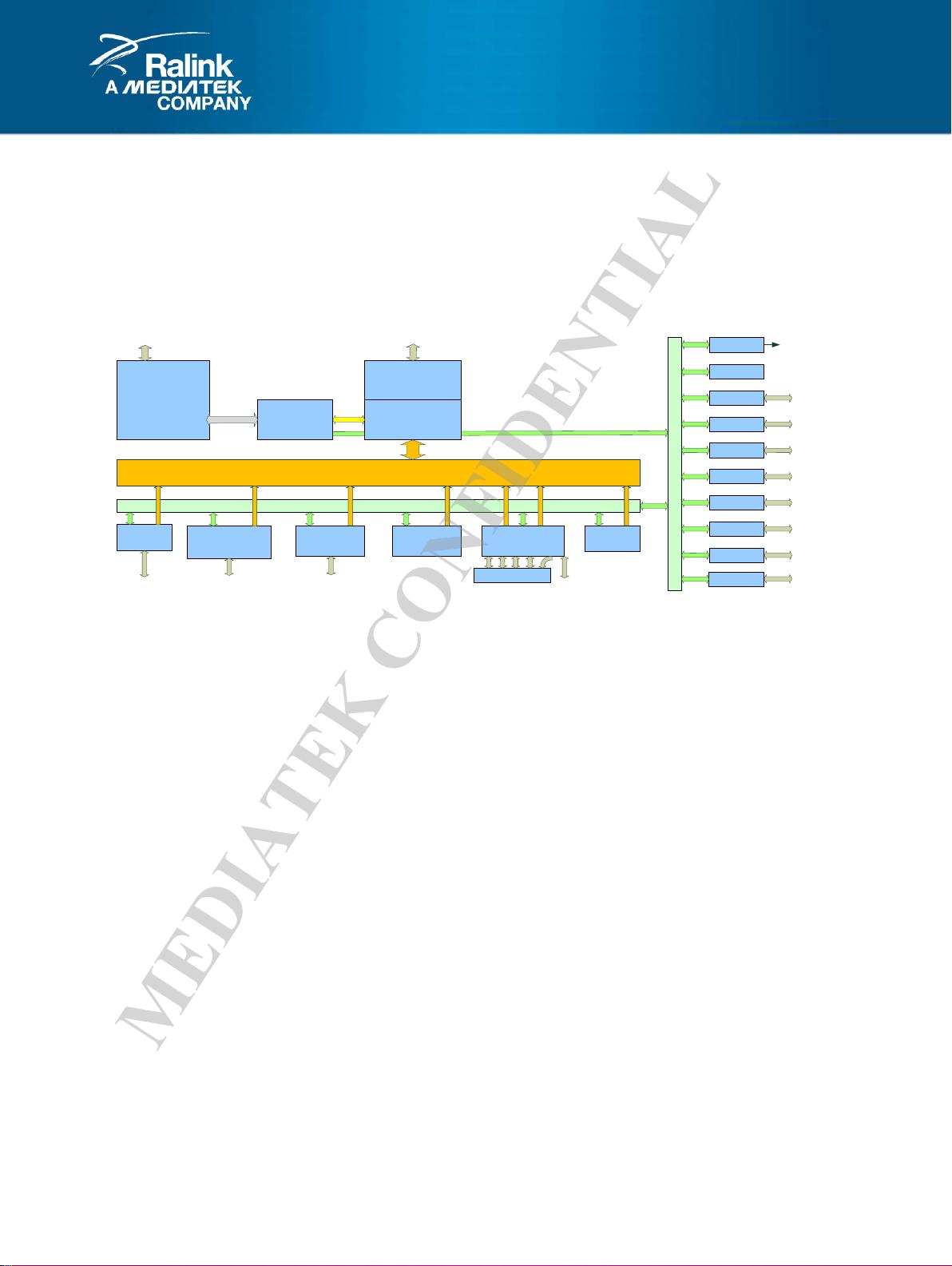
1. MIPS 1004Kc Processor
1.1 Features
8-9-stage pipeline
32-bit Address Paths
64-bit Data Paths to Caches
MIPS32 Enhanced Architecture (Release 2) Features
– Standardized Instruction Set Architecture
– Vectored interrupts and support for an external interrupt controller
– Programmable exception vector base
– Atomic interrupt enable/disable
– Bit field manipulation instructions
MIPS16e Application Specific Extension
– 16 bit encodings of 32-bit instructions to improve code density
– Special PC-relative instructions for efficient loading of addresses and constants
– Data type conversion instructions (ZEB, SEB, ZEH, SEH)
– Compact jumps (JRC, JALRC)
– Stack frame set-up and tear down “macro” instructions (SAVE and RESTORE)
MIPS MT Application Specific Extension (ASE)
– Support for 2 Virtual Processing Elements (VPEs) per CORE
– One Thread Context (TC) per VPE
Programmable L1 Cache Sizes
– Individually configurable instruction and data caches
– 32KB I/D cache
– 4-way set associative
– Up to 9 non-blocking loads
– Data cache supports coherent and non-coherent Write-back with write-allocation
– 32-byte cache line size, doubleword sectored - suitable for standard single-port SRAM
– Cache line locking support
– Non-blocking prefetches
– Duplicate tag array in D-cache allows coherence requests to access the cache in parallel with normal
load/store traffic
Standard Memory Management Unit
– 32 dual-entry MIPS32-style JTLB per VPE with variable page sizes
– JTLBs are sharable under software control
– 4-5 entry instruction TLB
– 8-entry data TLB
OCP Bus Interface Unit (BIU)
– 32b address and 64b data
– Supports bursts of 4x64b
– 8 entry write buffer - handles eviction data, intervention response, uncached, and uncached
accelerated store data
– Simple Byte enable mode allows easier bridging to other bus standards
– Extensions for management of front side L2 cache
– Intervention port supports memory coherency for use in a 1004K Coherent Processing System
Multiply-Divide Unit
– Maximum issue rate of one 32x32 multiply per clock
– Early-in divide control. Minimum 11, maximum 34 clock latency on divide
Power Control
– No minimum frequency
– Support for software-controlled clock divider
– Support for extensive use of fine-grain clock gating
MEDIATEK CONFIDENTIAL
剩余348页未读,继续阅读


安全验证
文档复制为VIP权益,开通VIP直接复制

评论0