
Copyright © Cirrus Logic, Inc. 2005
(All Rights Reserved)
http://www.cirrus.com
CS5463
Single Phase, Bi-directional Power/Energy IC
Features
z Energy Data Linearity: ±0.1% of Reading
over 1000:1 Dynamic Range
z On-chip Functions:
- Instantaneous Voltage, Current, and Power
- I
RMS
and V
RMS
, Apparent, Reactive, and Active
(Real) Power
- Active Fundamental and Harmonic Power
- Reactive Fundamental, Power Factor, and Line
Frequency
- Energy-to-pulse Conversion
- System Calibrations and Phase Compensation
- Temperature Sensor
z
Meets accuracy spec for IEC, ANSI, JIS.
z Low Power Consumption
z Current Input Optimized for Sense Resistor.
z GND-referenced Signals with Single Supply
z On-chip 2.5 V Reference (25 ppm/°C typ)
z Power Supply Monitor
z Simple Three-wire Digital Serial Interface
z “Auto-boot” Mode from Serial E
2
PROM
z Power Supply Configurations:
VA+ = +5 V; AGND = 0 V; VD+ = +3.3 V to +5 V
Description
The CS5463 is an integrated power measure-
ment device which combines two ∆Σ
analog-to-digital converters, power calculation
engine, energy-to-frequency converter, and a
serial interface on a single chip. It is designed to
accurately measure instantaneous current and
voltage, and calculate V
RMS
, I
RMS
, instanta-
neous power, apparent power, active power, and
reactive power for single-phase, 2- or 3-wire
power metering applications.
The CS5463 is optimized to interface to shunt re-
sistors or current transformers for current
measurement, and to resistive dividers or poten-
tial transformers for voltage measurement.
The CS5463 features a bi-directional serial inter-
face for communication with a processor and a
programmable energy-to-pulse output function.
Additional features include on-chip functionality
to facilitate system-level calibration, temperature
sensor, voltage sag detection, and phase
compensation.
ORDERING INFORMATION:
See Page 44.
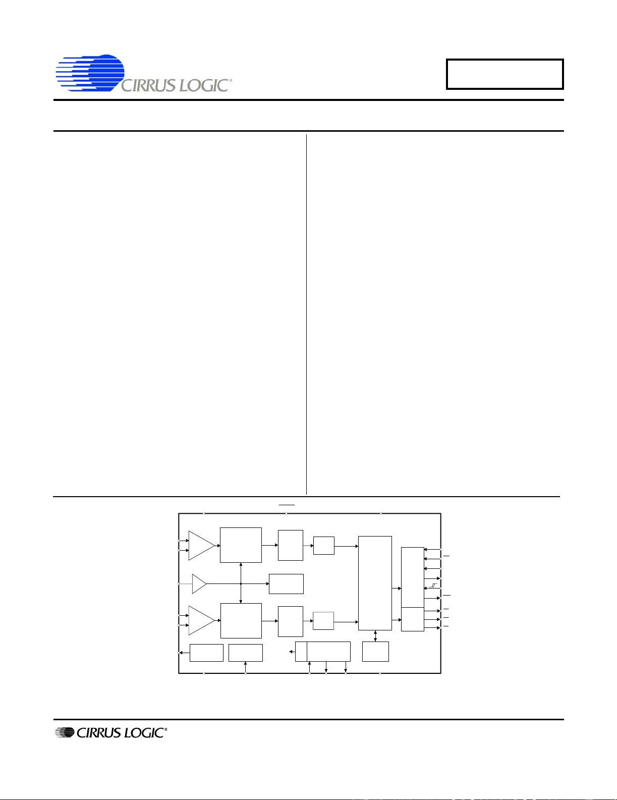
VA+ VD+
IIN+
IIN-
VIN+
VIN-
VREFIN
VREFOUT
AGND
XIN XOUT CPUCLK DGND
CS
SDO
SDI
SCLK
INT
Voltage
Reference
System
Clock
/K
Clock
Generat or
Serial
Interface
E-to-F
Power
Moni tor
PFMON
x1
RESET
Digital
Filter
Cal ibr ati on
MODE
Power
Calculation
Engine
4th Order ∆Σ
Modulator
2nd Order ∆Σ
Modulator
Temperature
Sensor
Digital
Filter
PGA
HPF
Option
HPF
Option
E1
E2
E3
x10
AUG ‘05
DS678PP1


剩余43页未读,继续阅读

guanxizhu
- 粉丝: 0
- 资源: 5
 我的内容管理
收起
我的内容管理
收起
- 我的资源
快来上传第一个资源
 我的收益 登录查看自己的收益
 我的积分
登录查看自己的积分
我的积分
登录查看自己的积分
 我的C币
登录后查看C币余额
我的C币
登录后查看C币余额
 我的收藏
我的收藏  我的下载
我的下载  下载帮助
下载帮助

会员权益专享


最新资源
- c++校园超市商品信息管理系统课程设计说明书(含源代码) (2).pdf
- 建筑供配电系统相关课件.pptx
- 企业管理规章制度及管理模式.doc
- vb打开摄像头.doc
- 云计算-可信计算中认证协议改进方案.pdf
- [详细完整版]单片机编程4.ppt
- c语言常用算法.pdf
- c++经典程序代码大全.pdf
- 单片机数字时钟资料.doc
- 11项目管理前沿1.0.pptx
- 基于ssm的“魅力”繁峙宣传网站的设计与实现论文.doc
- 智慧交通综合解决方案.pptx
- 建筑防潮设计-PowerPointPresentati.pptx
- SPC统计过程控制程序.pptx
- SPC统计方法基础知识.pptx
- MW全能培训汽轮机调节保安系统PPT教学课件.pptx
资源上传下载、课程学习等过程中有任何疑问或建议,欢迎提出宝贵意见哦~我们会及时处理!
点击此处反馈


评论0