没有合适的资源?快使用搜索试试~ 我知道了~
首页ADAU1701数据手册
资源详情
资源评论
资源推荐
SigmaDSP 28-/56-Bit Audio Processor
with Two ADCs and Four DACs
ADAU1701
Rev. B
Information furnished by Analog Devices is believed to be accurate and reliable. However, no
responsibility is assumed by Analog Devices for its use, nor for any infringements of patents or other
rights of third parties that may result from its use. Specifications subject to change without notice. No
license is granted by implication or otherwise under any patent or patent rights of Analog Devices.
Trademarks and registered trademarks are the property of their respective owners.
One Technology Way, P.O. Box 9106, Norwood, MA 02062-9106, U.S.A.
Tel: 781.329.4700 www.analog.com
Fax: 781.461.3113 ©2007–2011 Analog Devices, Inc. All rights reserved.
FEATURES
28-/56-bit, 50 MIPS digital audio processor
2 ADCs: SNR of 100 dB, THD + N of −83 dB
4 DACs: SNR of 104 dB, THD + N of −90 dB
Complete standalone operation
Self-boot from serial EEPROM
Auxiliary ADC with 4-input mux for analog control
GPIOs for digital controls and outputs
Fully programmable with SigmaStudio graphical tool
28-bit × 28-bit multiplier with 56-bit accumulator for full
double-precision processing
Clock oscillator for generating a master clock from crystal
PLL for generating master clock from 64 × f
S
, 256 × f
S
,
384 × f
S
, or 512 × f
S
clocks
Flexible serial data input/output ports with I
2
S-compatible,
left-justified, right-justified, and TDM modes
Sampling rates of up to 192 kHz are supported
On-chip voltage regulator for compatibility with 3.3 V systems
48-lead, plastic LQFP
APPLICATIONS
Multimedia speaker systems
MP3 player speaker docks
Automotive head units
Minicomponent stereos
Digital televisions
Studio monitors
Speaker crossovers
Musical instrument effects processors
In-seat sound systems (aircraft/motor coaches)
GENERAL DESCRIPTION
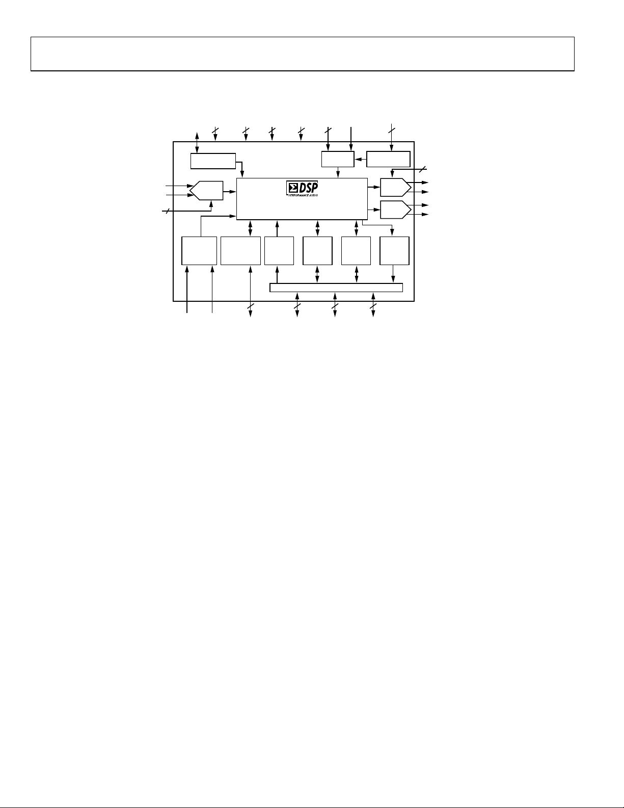
The ADAU1701 is a complete single-chip audio system with a
28-/56-bit audio DSP, ADCs, DACs, and microcontroller-like
control interfaces. Signal processing includes equalization, cross-
over, bass enhancement, multiband dynamics processing, delay
compensation, speaker compensation, and stereo image widening.
This processing can be used to compensate for real-world
limitations of speakers, amplifiers, and listening environments,
providing dramatic improvements in perceived audio quality.
Its signal processing is comparable to that found in high end
studio equipment. Most processing is done in full 56-bit, double
precision mode, resulting in very good low level signal perfor-
mance. The ADAU1701 is a fully programmable DSP. The easy to
use SigmaStudio™ software allows the user to graphically configure
a custom signal processing flow using blocks such as biquad filters,
dynamics processors, level controls, and GPIO interface controls.
ADAU1701 programs can be loaded on power-up either from a
serial EEPROM through its own self-boot mechanism or from
an external microcontroller. On power-down, the current state
of the parameters can be written back to the EEPROM from the
ADAU1701 to be recalled the next time the program is run.
Two Σ-Δ ADCs and four Σ-Δ DACs provide a 98.5 dB analog
input to analog output dynamic. Each ADC has a THD + N of
−83 dB, and each DAC has a THD + N of −90 dB. Digital input
and output ports allow a glueless connection to additional
ADCs and DACs. The ADAU1701 communicates through an
I
2
C® bus or a 4-wire SPI port.
ADAU1701
Rev. B | Page 2 of 52
TABLE OF CONTENTS
Features .............................................................................................. 1
Applications....................................................................................... 1
General Description......................................................................... 1
Revision History ............................................................................... 3
Functional Block Diagram .............................................................. 4
Specifications..................................................................................... 5
Analog Performance .................................................................... 5
Digital Input/Output.................................................................... 6
Power.............................................................................................. 6
Temperature Range ...................................................................... 6
PLL and Oscillator........................................................................ 6
Regulator........................................................................................ 7
Digital Timing Specifications ..................................................... 7
Absolute Maximum Ratings.......................................................... 10
Thermal Resistance .................................................................... 10
ESD Caution................................................................................ 10
Pin Configuration and Function Descriptions........................... 11
Typical Performance Characteristics ........................................... 14
System Block Diagram................................................................... 15
Theory of Operation ...................................................................... 16
Initialization .................................................................................... 17
Power-Up Sequence ................................................................... 17
Control Registers Setup ............................................................. 17
Recommended Program/Parameter Loading Procedure ..... 17
Power Reduction Modes............................................................ 17
Using the Oscillator.................................................................... 18
Setting Master Clock/PLL Mode.............................................. 18
Voltage Regulator ....................................................................... 19
Audio ADCs .................................................................................... 20
Audio DACs .................................................................................... 21
Control Ports................................................................................... 22
I
2
C Port ........................................................................................ 23
SPI Port ........................................................................................ 26
Self-Boot ...................................................................................... 27
Signal Processing ............................................................................ 29
Numeric Formats........................................................................ 29
Programming .............................................................................. 29
RAMs and Registers....................................................................... 30
Address Maps.............................................................................. 30
Parameter RAM.......................................................................... 30
Data RAM ................................................................................... 30
Read/Write Data Formats ......................................................... 30
Control Register Map..................................................................... 32
Control Register Details ................................................................ 34
2048 to 2055 (0x0800 to 0x0807)—Interface Registers......... 34
2056 (0x0808)—GPIO Pin Setting Register ........................... 35
2057 to 2060 (0x0809 to 0x080C)—Auxiliary ADC Data
Registers....................................................................................... 36
2064 to 2068 (0x0810 to 0x0814)—Safeload Data Registers 37
2069 to 2073 (0x0815 to 0x819)—Safeload Address Registers
....................................................................................................... 37
2074 to 2075 (0x081A to 0x081B)—Data Capture Registers 38
2076 (0x081C)—DSP Core Control Register ......................... 39
2078 (0x081E)—Serial Output Control Register ................... 40
2079 (0x081F)—Serial Input Control Register....................... 41
2080 to 2081 (0x0820 to 0x0821)—Multipurpose Pin
Configuration Registers............................................................. 42
2082 (0x0822)—Auxiliary ADC and Power Control ............ 43
2084 (0x0824)—Auxiliary ADC Enable.................................. 43
2086 (0x0826)—Oscillator Power-Down................................ 43
2087 (0x0827)—DAC Setup...................................................... 44
Multipurpose Pins .......................................................................... 45
Auxiliary ADC............................................................................ 45
General-Purpose Input/Output Pins....................................... 45
Serial Data Input/Output Ports ................................................ 45
Layout Recommendations............................................................. 48
Parts Placement .......................................................................... 48
Grounding ................................................................................... 48
Typical Application Schematics.................................................... 49
Self-Boot Mode........................................................................... 49
I
2
C Control .................................................................................. 50
SPI Control.................................................................................. 51
Outline Dimensions ....................................................................... 52
Ordering Guide .......................................................................... 52
ADAU1701
Rev. B | Page 3 of 52
REVISION HISTORY
6/11—Rev. A to Rev. B
Deleted Table 2; Renumbered Sequentially ...................................6
Changes to Table 4 ............................................................................
6
2/11—Re
v. 0 to Rev. A
Moved Figure 1..................................................................................4
Changes to Specifications Section...................................................5
Changes to Table 8, Test Conditions/Comments Column ..........8
Reordered Figures in Digital Timing Diagrams Section .............9
Changes to Figure 2...........................................................................9
Changes to Figure 5 and Figure 6..................................................10
Changes to Table 11 ........................................................................12
Replaced Figure 8 to Figure 11 ......................................................15
Renamed Theory of Operation Section .......................................17
Changes to Initialization Section ..................................................18
Change to Setting the Master Clock/PLL Mode Section ...........19
Changes to Table 15 ........................................................................23
Replaced Figure 22 through Figure 25 .........................................26
Changes to EEPROM Format Section..........................................28
Deleted Table 20, Renumbered Sequentially...............................29
Inserted Figure 28, Renumbered Sequentially ............................29
Changes to Control Register Details Section...............................35
Changes to Ordering Guide...........................................................53
7/07—Revision 0: Initial Version
ADAU1701
Rev. B | Page 4 of 52
FUNCTIONAL BLOCK DIAGRAM
2
2
GPIO
INPUT/OUTPUT MATRIX
DIGITAL
VDD
DIGITAL
GROUND
A
NALOG
VDD
A
NALOG
GROUND
PLL
MODE
PLL LOOP
FILTER
CRYSTAL
3.3V
28-/56-BIT, 50MIPS
AUDIO PROCESSOR CORE
40ms DELAY MEMORY
2-CHANNEL
ANALOG
INPUT
1.8V
REGULATOR
STEREO
ADC
FILTA/
ADC_RES
RESET/
MODE
SELECT
CONTROL
INTERFACE
AND
SELFBOOT
8-CH
DIGITAL
INPUT
8-CH
DIGITAL
OUTPUT
8-BIT
AUX
ADC
RESET
SELFBOOT
DIGITAL IN
OR GPIO
AUX ADC
OR GPIO
DIGITAL OUT
OR GPIO
I
2
C/SPI
AND WRITEBACK
DAC
DAC
4-CHANNEL
ANALOG
OUTPUT
FILTD/CM
PLL
CLOCK
OSCILLATOR
ADAU1701
3 3 3 2 22
3335
0
6412-001
Figure 1.
ADAU1701
Rev. B | Page 5 of 52
SPECIFICATIONS
AVDD = 3.3 V, DVDD = 1.8 V, PVDD = 3.3 V, IOVDD = 3.3 V, master clock input = 12.288 MHz, unless otherwise noted.
ANALOG PERFORMANCE
Specifications are guaranteed at 25°C (ambient).
Table 1.
Parameter Min Typ Max Unit Test Conditions/Comments
ADC INPUTS
Number of Channels 2 Stereo input
Resolution 24 Bits
Full-Scale Input 100 (283) µA rms (µA p-p)
2 V rms input with 20 kΩ (18 kΩ external + 2 kΩ
internal) series resistor
Signal-to-Noise Ratio
A-Weighted 100 dB
Dynamic Range −60 dB with respect to full-scale analog input
A-Weighted 95 100 dB
Total Harmonic Distortion + Noise −83 dB −3 dB with respect to full-scale analog input
Interchannel Gain Mismatch 25 250 mdB
Crosstalk −82 dB Analog channel-to-channel crosstalk
DC Bias 1.4 1.5 1.6 V
Gain Error −11 +11 %
DAC OUTPUTS
Number of Channels 4 Two stereo output channels
Resolution 24 Bits
Full-Scale Analog Output 0.9 (2.5) V rms (V p-p)
Signal-to-Noise Ratio
A-Weighted 104 dB
Dynamic Range −60 dB with respect to full-scale analog output
A-Weighted 99 104 dB
Total Harmonic Distortion + Noise −90 dB −1 dB with respect to full-scale analog output
Crosstalk −100 dB Analog channel-to-channel crosstalk
Interchannel Gain Mismatch 25 250 mdB
Gain Error −10 +10 %
DC Bias 1.4 1.5 1.6 V
VOLTAGE REFERENCE
Absolute Voltage (CM) 1.4 1.5 1.6 V
AUXILIARY ADC
Full-Scale Analog Input 2.8 3.0 3.1 V
INL 0.5 LSB
DNL 1.0 LSB
Offset 15 mV
Input Impedance 17.8 30 42 kΩ
剩余51页未读,继续阅读
尘草
- 粉丝: 0
- 资源: 4
上传资源 快速赚钱
- 我的内容管理 收起
- 我的资源 快来上传第一个资源
- 我的收益 登录查看自己的收益
- 我的积分 登录查看自己的积分
- 我的C币 登录后查看C币余额
- 我的收藏
- 我的下载
- 下载帮助
会员权益专享
最新资源
- 27页智慧街道信息化建设综合解决方案.pptx
- 计算机二级Ms-Office选择题汇总.doc
- 单链表的插入和删除实验报告 (2).docx
- 单链表的插入和删除实验报告.pdf
- 物联网智能终端项目设备管理方案.pdf
- 如何打造品牌的模式.doc
- 样式控制与页面布局.pdf
- 武汉理工Java实验报告(二).docx
- 2021线上新品消费趋势报告.pdf
- 第3章 Matlab中的矩阵及其运算.docx
- 基于Web的人力资源管理系统的必要性和可行性.doc
- 基于一阶倒立摆的matlab仿真实验.doc
- 速运公司物流管理模式研究教材
- 大数据与管理.pptx
- 单片机课程设计之步进电机.doc
- 大数据与数据挖掘.pptx
资源上传下载、课程学习等过程中有任何疑问或建议,欢迎提出宝贵意见哦~我们会及时处理!
点击此处反馈
安全验证
文档复制为VIP权益,开通VIP直接复制
信息提交成功
评论0