Apollo Datasheet
Ultra-Low Power MCU Family
Ambiq Micro Inc. 6500 River Place Blvd., Bldg. 7, Ste. 200 2016 Ambiq Micro, Inc.
www.ambiqmicro.com Austin, TX 78730-1156 February 2016
Ambiq Micro
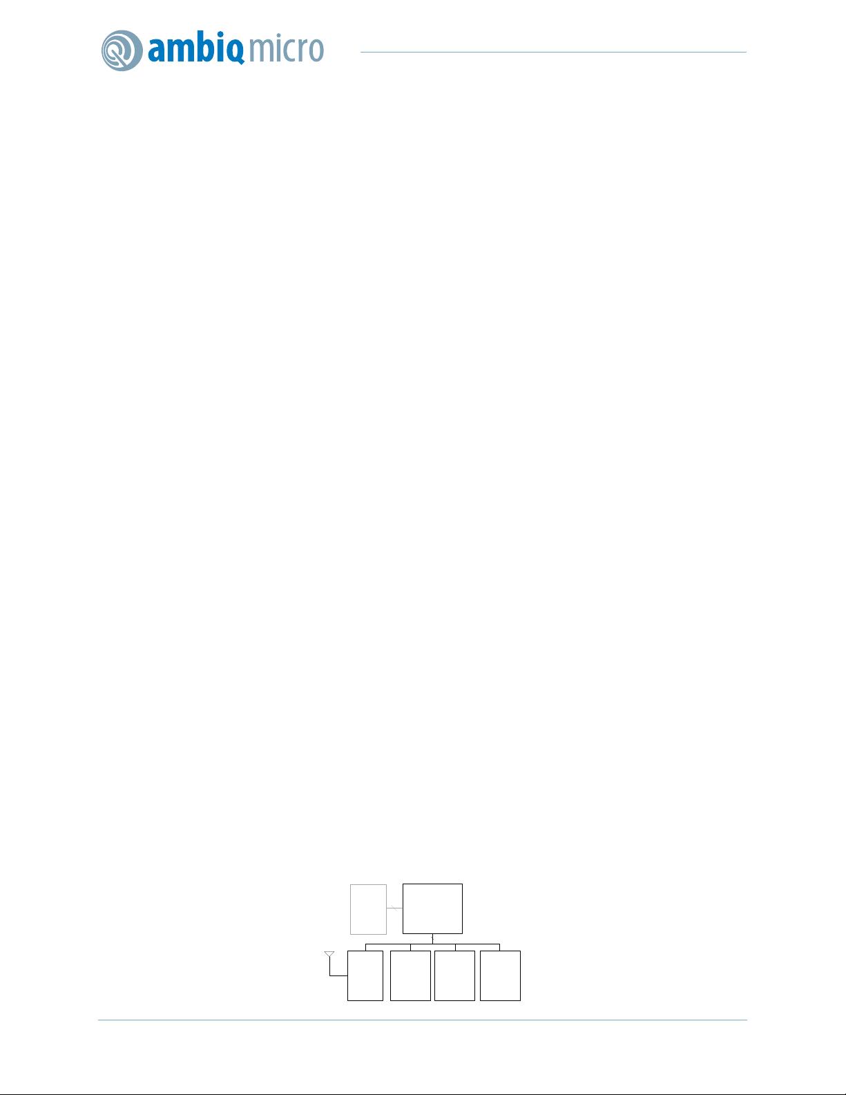
Apollo
MCU
Host
Processor
(optional)
SPI/I
2
C
Slave
Port
SPI/I
2
C Master,
UART
Radio
Magnetometer
with Digital
Output
Gyroscope
with Digital
Output
Accelerometer
with Digital
Output
Typical Sensor Application Circuit for the Apollo MCU
Features
Ultra-low supply current:
- EEMBC ULPBench score of 377
- 35 µA/MHz executing from flash at 3.3 V
- 143 nA deep sleep mode at 3.3 V
- 419 nA deep sleep mode with XTAL-assisted
RTC at 3.3 V
High-performance ARM Cortex-M4F Processor
- Up to 24 MHz clock frequency
- Floating point unit
- Memory protection unit
Wake-up interrupt controller with 12 interrupts
Ultra-low power memory:
- Up to 512 KB of flash memory for code/data
- Up to 64 KB of low leakage RAM for code/data
Ultra-low power interface for off-chip sensors:
- 10 bit, 13-channel, up to 800 kSps ADC
- Temperature sensor with +/-4ºC accuracy
Flexible serial peripherals:
-I
2
C/SPI master for communication with sensors,
radios, and other peripherals
-I
2
C/SPI slave for host communications
- UART for communication with peripherals and
legacy devices
Rich set of clock sources:
- 32.768 kHz XTAL oscillator
- Low frequency RC oscillator – 1.024 kHz
- High frequency RC oscillator – 24 MHz
- RTC based on Ambiq’s AM08X5/18X5 families
Wide operating range: 1.8-3.8 V, –40 to 85°C
Compact package options:
- 2.49 x 2.90 mm 41-pin CSP with 27 GPIO
- 4.5 x 4.5 mm 64-pin BGA with 50 GPIO
Applications
- Wearable electronics
- Wireless sensors
- Activity and fitness monitors
- Consumer electronics
- Consumer medical devices
- Smart watches
Description
The Apollo MCU family is an ultra-low power, highly
integrated microcontroller designed for battery-
powered devices including wearable electronics,
activity & fitness monitors, and wireless sensors. By
combining ultra-low power sensor conversion
electronics with the powerful ARM Cortex-M4F
processor, the Apollo MCU enables complex sensor
processing tasks to be completed with
unprecedented battery life. Weeks, months, and
years of battery life are achievable while doing
complex context detection, gesture recognition, and
activity monitoring. The Apollo MCU takes full
advantage of Ambiq Micro’s patented Subthreshold
Power Optimized Technology (SPOT) Platform,
setting a new industry benchmark in low power
design.
The Apollo MCU also integrates up to 512 KB of
flash memory and 64 KB of RAM to accommodate
radio and sensor overhead while still leaving plenty
of space for application code. This microcontroller
also includes a serial master and UART port for
communicating with radios and sensors including
accelerometers, gyroscopes, and magnetometers.


剩余383页未读,继续阅读

foolishlee
- 粉丝: 12
- 资源: 58
 我的内容管理
收起
我的内容管理
收起
- 我的资源
快来上传第一个资源
 我的收益 登录查看自己的收益
 我的积分
登录查看自己的积分
我的积分
登录查看自己的积分
 我的C币
登录后查看C币余额
我的C币
登录后查看C币余额
 我的收藏
我的收藏  我的下载
我的下载  下载帮助
下载帮助

会员权益专享


最新资源
- stc12c5a60s2 例程
- Android通过全局变量传递数据
- c++校园超市商品信息管理系统课程设计说明书(含源代码) (2).pdf
- 建筑供配电系统相关课件.pptx
- 企业管理规章制度及管理模式.doc
- vb打开摄像头.doc
- 云计算-可信计算中认证协议改进方案.pdf
- [详细完整版]单片机编程4.ppt
- c语言常用算法.pdf
- c++经典程序代码大全.pdf
- 单片机数字时钟资料.doc
- 11项目管理前沿1.0.pptx
- 基于ssm的“魅力”繁峙宣传网站的设计与实现论文.doc
- 智慧交通综合解决方案.pptx
- 建筑防潮设计-PowerPointPresentati.pptx
- SPC统计过程控制程序.pptx
资源上传下载、课程学习等过程中有任何疑问或建议,欢迎提出宝贵意见哦~我们会及时处理!
点击此处反馈


评论1