没有合适的资源?快使用搜索试试~ 我知道了~
首页Beken BK2425 datasheet
Beken BK2425 datasheet
需积分: 47 21 下载量 116 浏览量
更新于2023-03-16
评论
收藏 454KB PDF 举报
BK2425是博通集成电路BK24xx系列2.4GHz收发器和系统芯片(SoC)系列产品中的新成员 1、该系列可提供从250 kbps到4 Mbps的无线数据速率 2、BK2425与该公司大受欢迎的BK2423 GFSK收发器引脚兼容 3、广泛应用于无线键盘/鼠标、无线音频、无线游戏控制器/游戏键盘 4、无线安全、家庭自动化和工业控制等众多应用中 5、BK2425自身可提供+5 dBm的输出功率 6、而通过简单的50欧姆PCB布局修改将RFX2401C嵌入到BK2425射频引脚和天线端口之间后 7、则可提供多达+20 dBm的最大传输功率,同时还能在接收灵敏度方面实现重大改进。
资源详情
资源评论
资源推荐
BK2425
Revision 1.0 Copyright © 2013 Beken Corporation
Jan, 2013 Page 1 of 30
Low Power High Performance 2.4 GHz GFSK Transceiver
Features
2400-2483.5 MHz ISM band operation
Support 250Kbps, 1Mbps and 2 Mbps air
data rate
Programmable output power
Low power consumption
Tolerate +/- 60ppm 16 MHz crystal
Variable payload length from 1 to 32bytes
Automatic packet processing
6 data pipes for 1:6 star networks
1.9V to 3.6V power supply
4-pin SPI interface with maximum 8 MHz
clock rate
20-pin 4x4mm QFN package
Applications
Wireless PC peripherals
Wireless gamepads
Wireless audio
Remote controls
Home automation
Toys
Block Diagram
Pin Assignments
1
2
3
4
5
BK2425
6 7 8 109
14
13
12
11
NC
NC
NC
CE
CSN VSS
RF
NC CDVDD VDD
NC
15
1617181920
SCK
MOS I
MI S O
IRQ XO XI
VSS VDD
VDD
Integrated
TDD RF
Transceiver
XTALNXTALP
FM
Demodulator
FM Modulator
Data Slicer
Rx FIFO
Tx FIFO
Gaussian
shaping
Packet
Processing &
State Control
SPI
Interface
Power
Management
CE
IRQ
CSN
SCK
MOSI
MISO
RFP
RFN
Register
banks
BK2425
Revision 1.0 Proprietary and Confidential Page 2 of 30
Table of Contents
1 General Description ................................................................................................................. 3
2 Abbreviations .......................................................................................................................... 4
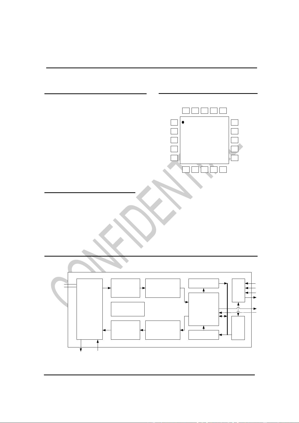
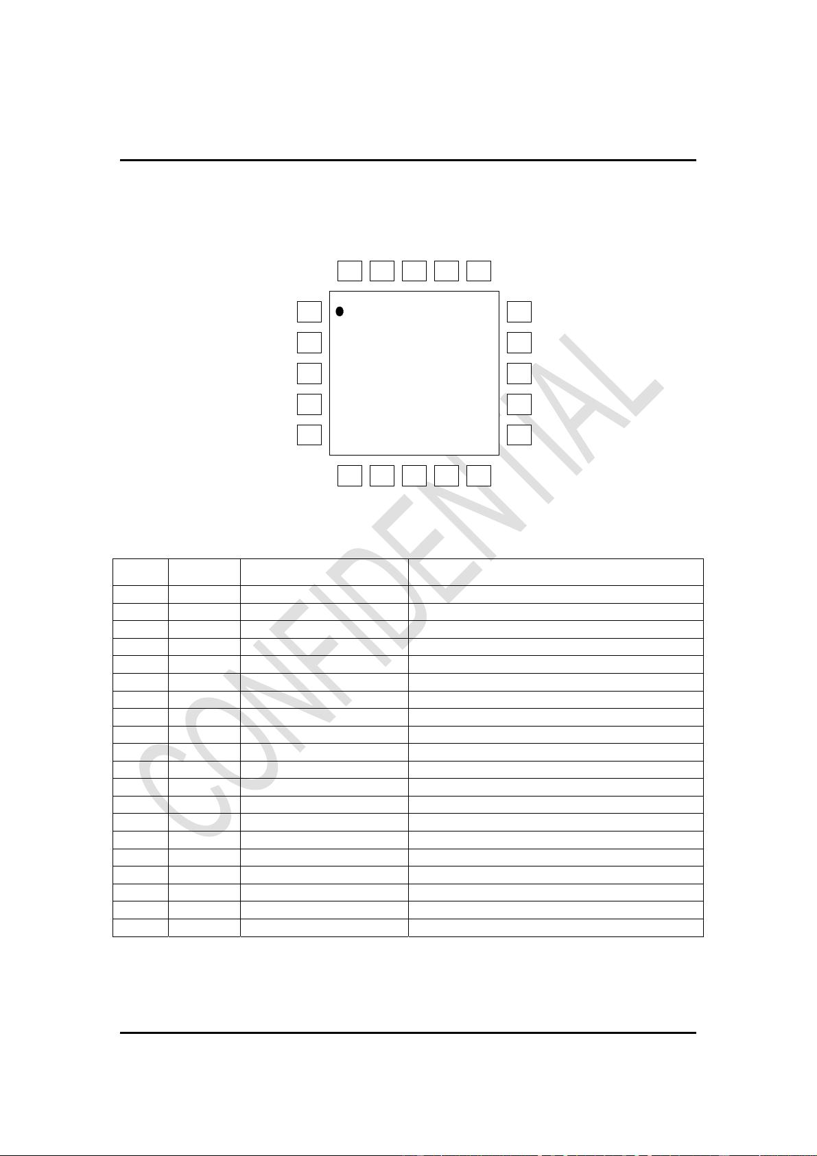
3 Pin Information ....................................................................................................................... 5
4 State Control ........................................................................................................................... 6
4.1 State Control Diagram ............................................................................................................... 6
4.2 Power Down Mode .................................................................................................................... 7
4.3 Standby-I Mode ......................................................................................................................... 7
4.4 Standby-II Mode ........................................................................................................................ 7
4.5 TX Mode ................................................................................................................................... 7
4.6 RX Mode ................................................................................................................................... 8
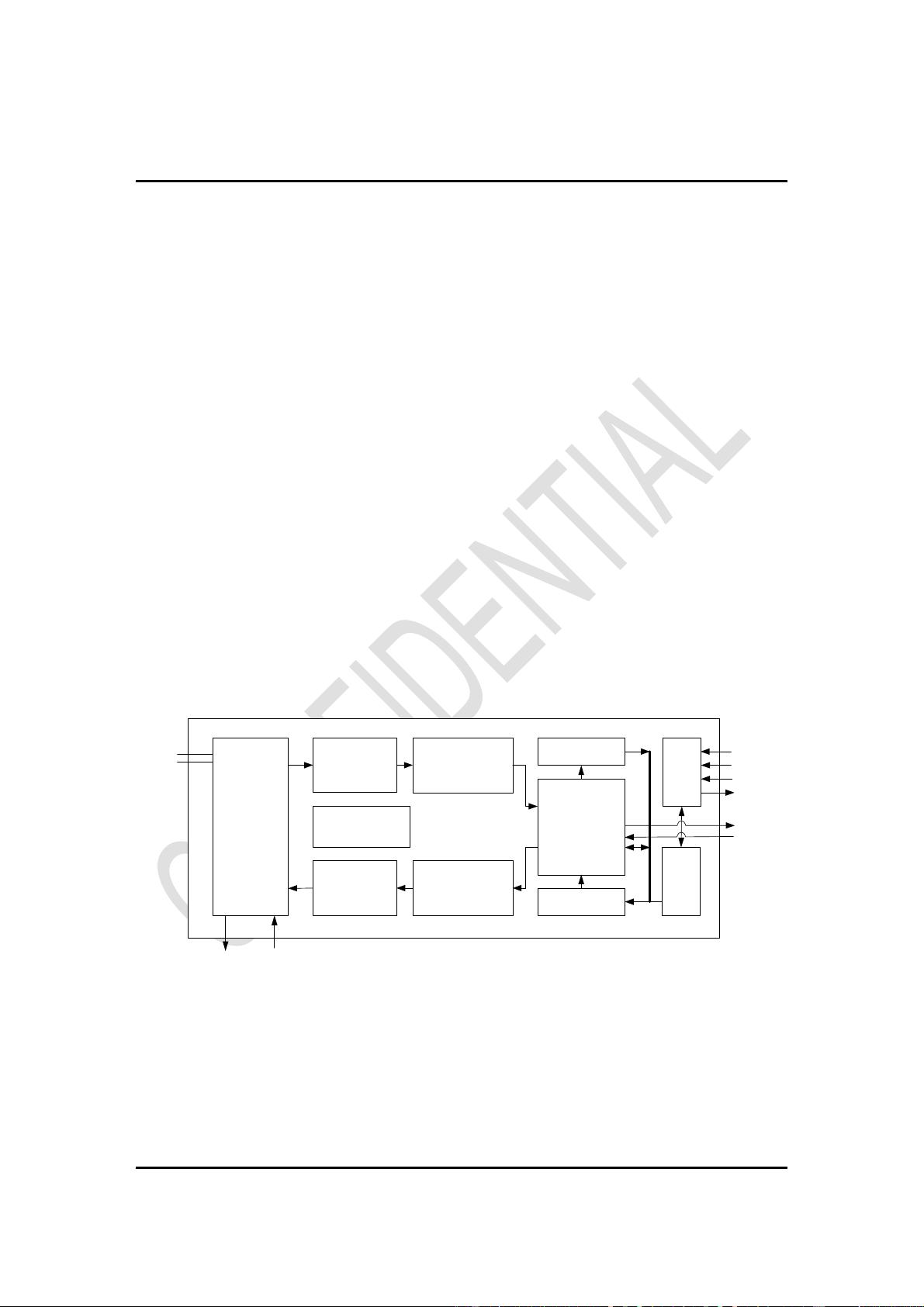
5 Packet Processing .................................................................................................................... 8
5.1 Packet Format ............................................................................................................................ 8
5.1.1 Preamble ........................................................................................................................... 9
5.1.2 Address ............................................................................................................................. 9
5.1.3 Packet Control .................................................................................................................. 9
5.1.4 Payload ........................................................................................................................... 10
5.1.5 CRC ................................................................................................................................ 10
5.2 Packet Handling ...................................................................................................................... 10
6 Data and Control Interface .................................................................................................... 11
6.1 TX/RX FIFO ........................................................................................................................... 11
6.2 Interrupt ................................................................................................................................... 11
6.3 SPI Interface ............................................................................................................................ 12
6.3.1 SPI Command ................................................................................................................ 12
6.3.2 SPI Timing ..................................................................................................................... 13
7 Register Map ......................................................................................................................... 15
7.1 Register Bank 0 ....................................................................................................................... 15
7.2 Register Bank 1 ....................................................................................................................... 21
8 Electrical Specifications ......................................................................................................... 22
9 Typical Application Schematic ............................................................................................... 23
10 Package and Die Bonding Information ................................................................................... 24
10.1 Package Information ........................................................................................................... 24
10.2 Die Bonding Information .................................................................................................... 25
10.3 PCB Bonding diagram ........................................................................................................ 27
11 Order Information ................................................................................................................. 28
12 Contact Information .............................................................................................................. 29
13 Update History ...................................................................................................................... 30
BK2425
Revision 1.0 Proprietary and Confidential Page 3 of 30
1 General Description
BK2425 is a GFSK transceiver operating in
the world wide ISM frequency band at 2400-
2483.5 MHz. Burst mode transmission and up
to 2Mbps air data rate make them suitable for
applications requiring ultra low power
consumption. The embedded packet
processing engines enable their full operation
with a very simple MCU as a radio system.
Auto re-transmission and auto acknowledge
give reliable link without any MCU
interference.
BK2425 operates in TDD mode, either as a
transmitter or as a receiver.
The RF channel frequency determines the
center of the channel used by BK2425. The
frequency is set by the RF_CH register in
register bank 0 according to the following
formula: F0= 2400 + RF_CH (MHz). The
resolution of the RF channel frequency is
1MHz.
A transmitter and a receiver must be
programmed with the same RF channel
frequency to be able to communicate with
each other.
The output power of BK2425 is set by the
RF_PWR bits in the RF_SETUP register.
Demodulation is done with embedded data
slicer and bit recovery logic. The air data rate
can be programmed to 250Kbps, 1Mbps or
2Mbps by RF_DR_HIGH and RF_DR_LOW
register. A transmitter and a receiver must be
programmed with the same setting.
In the following chapters, all registers are in
register bank 0 except with explicit claim.
Figure 1 BK2425 Chip Block Diagram
Integrated
TDD RF
Transceiver
XTALNXTALP
FM
Demodulator
FM Modulator
Data Slicer
Rx FIFO
Tx FIFO
Gaussian
shaping
Packet
Processing &
State Control
SPI
Interface
Power
Management
CE
IRQ
CSN
SCK
MOSI
MISO
RFP
RFN
Register
banks
BK2425
Revision 1.0 Proprietary and Confidential Page 4 of 30
2 Abbreviations
ACK Acknowledgement
ARC Auto Retransmission Count
ARD Auto Retransmission Delay
CD Carrier Detection
CE Chip Enable
CRC Cyclic Redundancy Check
CSN Chip Select Not
DPL Dynamic Payload Length
FIFO First-In-First-Out
GFSK Gaussian Frequency Shift Keying
GHz Gigahertz
LNA Low Noise Amplifier
IRQ Interrupt Request
ISM Industrial-Scientific-Medical
LSB Least Significant Bit
MAX_RT Maximum Retransmit
Mbps Megabit per second
MCU Microcontroller Unit
MHz Megahertz
MISO Master In Slave Out
MOSI Master Out Slave In
MSB Most Significant Bit
PA Power Amplifier
PID Packet Identity Bits
PLD Payload
PRX Primary RX
PTX Primary TX
PWD_DWN Power Down
PWD_UP Power Up
RF_CH Radio Frequency Channel
RSSI Received Signal Strength Indicator
RX Receive
RX_DR Receive Data Ready
SCK SPI Clock
SPI Serial Peripheral Interface
TDD Time Division Duplex
TX Transmit
TX_DS Transmit Data Sent
XTAL Crystal
BK2425
Revision 1.0 Proprietary and Confidential Page 5 of 30
3 Pin Information
1
2
3
4
5
BK2425
6 7 8 109
14
13
12
11
NC
NC
NC
CE
CSN VSS
RF
NC CDVDD VDD
NC
15
1617181920
SCK
MOSI
MI SO
IRQ XO XI
VSS VDD
VDD
Figure 2
BK2425 pin assignments (top view) for the QFN20 package
PIN Name Pin Function Description
1
CE Digital Input Chip Enable Activates RX or TX mode
2
CSN Digital Input SPI Chip Select, Active low
3
SCK Digital Input SPI Clock
4
MOSI Digital Input SPI Slave Data Input
5
MISO Digital Output SPI Slave Data Output with tri-state option
6
IRQ Digital Output Maskable interrupt pin, Active low
7
NC
No Connection
8
NC
No Connection
9
XO Analog Output Crystal oscillator, node P (inverter output)
10
XI Analog Input Crystal oscillator, node N (inverter input)
11
NC
No Connection
12
NC
No Connection
13
RFN RF port RF output (PA) /Input (LNA), port N.
14
VSS Ground Ground (0 V)
15
VDD Power Power Supply (1.9 V to 3.6 V DC)
16
VDD
Power Supply (1.9 V to 3.6 V DC)
17
VSS Ground Ground (0 V)
18
VDD Power Power Supply (1.9 V to 3.6 V DC)
19
CDVDD Analog Output Digital regulator output decoupling capacitor
20
NC
No Connection
Table 1 BK2425 QFN20 pin functions
剩余29页未读,继续阅读
6+0的蜗牛
- 粉丝: 3
- 资源: 3
上传资源 快速赚钱
- 我的内容管理 收起
- 我的资源 快来上传第一个资源
- 我的收益 登录查看自己的收益
- 我的积分 登录查看自己的积分
- 我的C币 登录后查看C币余额
- 我的收藏
- 我的下载
- 下载帮助
会员权益专享
最新资源
- stc12c5a60s2 例程
- Android通过全局变量传递数据
- c++校园超市商品信息管理系统课程设计说明书(含源代码) (2).pdf
- 建筑供配电系统相关课件.pptx
- 企业管理规章制度及管理模式.doc
- vb打开摄像头.doc
- 云计算-可信计算中认证协议改进方案.pdf
- [详细完整版]单片机编程4.ppt
- c语言常用算法.pdf
- c++经典程序代码大全.pdf
- 单片机数字时钟资料.doc
- 11项目管理前沿1.0.pptx
- 基于ssm的“魅力”繁峙宣传网站的设计与实现论文.doc
- 智慧交通综合解决方案.pptx
- 建筑防潮设计-PowerPointPresentati.pptx
- SPC统计过程控制程序.pptx
资源上传下载、课程学习等过程中有任何疑问或建议,欢迎提出宝贵意见哦~我们会及时处理!
点击此处反馈
安全验证
文档复制为VIP权益,开通VIP直接复制
信息提交成功
评论0