© Semiconductor Components Industries, LLC, 2015
August, 2017 − Rev. 2
1 Publication Order Number:
FUSB302BCN/D
FUSB302B
采PD的编程USBType‐C
说
FUSB302B向期望实现DRP/SRC/SNK USB Type-C接器,
少程的员。
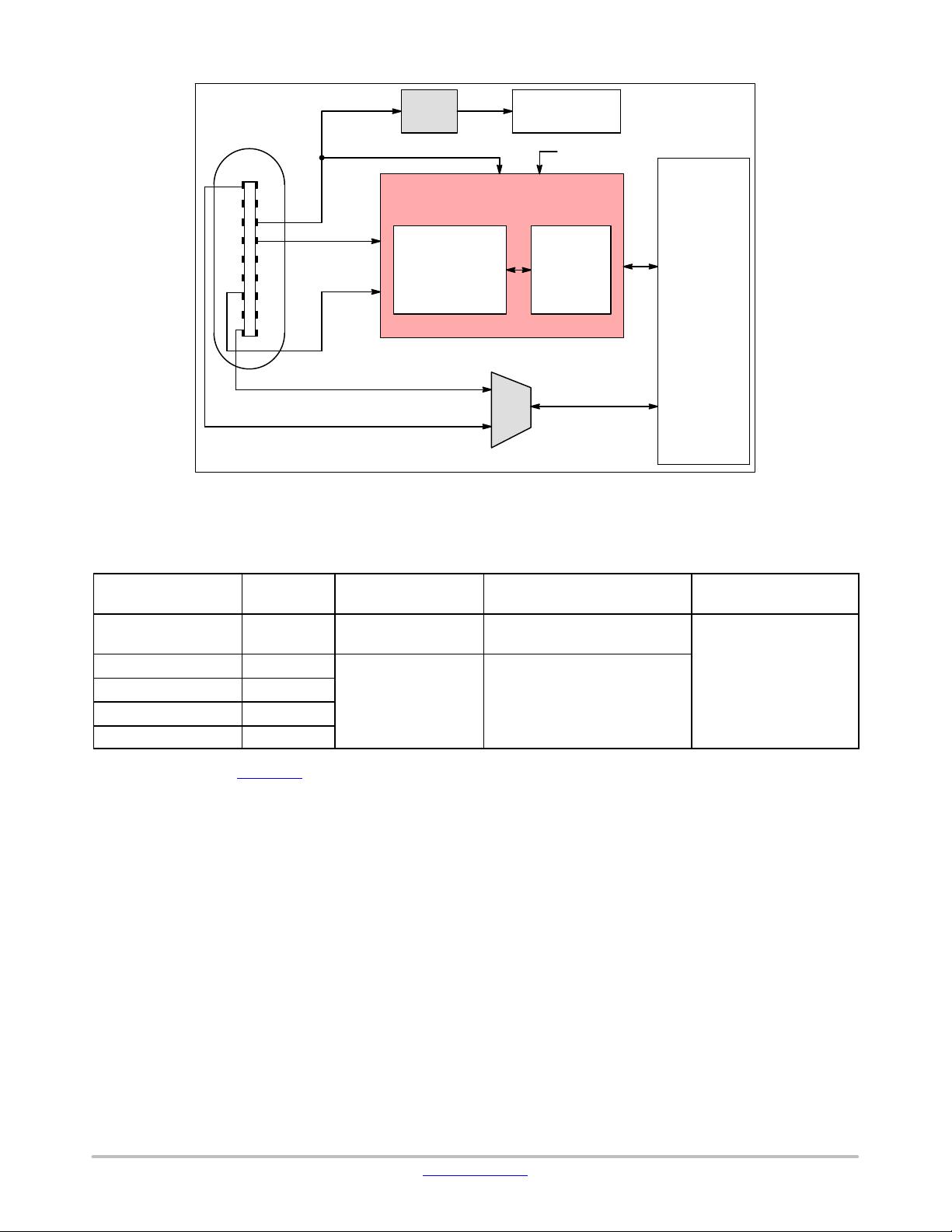
FUSB302B支持USB Type-C检测, 包括 接和方向。
FUSB302B成USB BMC电力协的物理层,
100 W功率和换。BMC的PD模块支持Type-C格的替
接口。
•动DRP切换的双功
•基接对可机或备接的力。
•可用机、用备或双。
♦用备可在带固定CC或VCONN 的Type-C插座或插
头!。
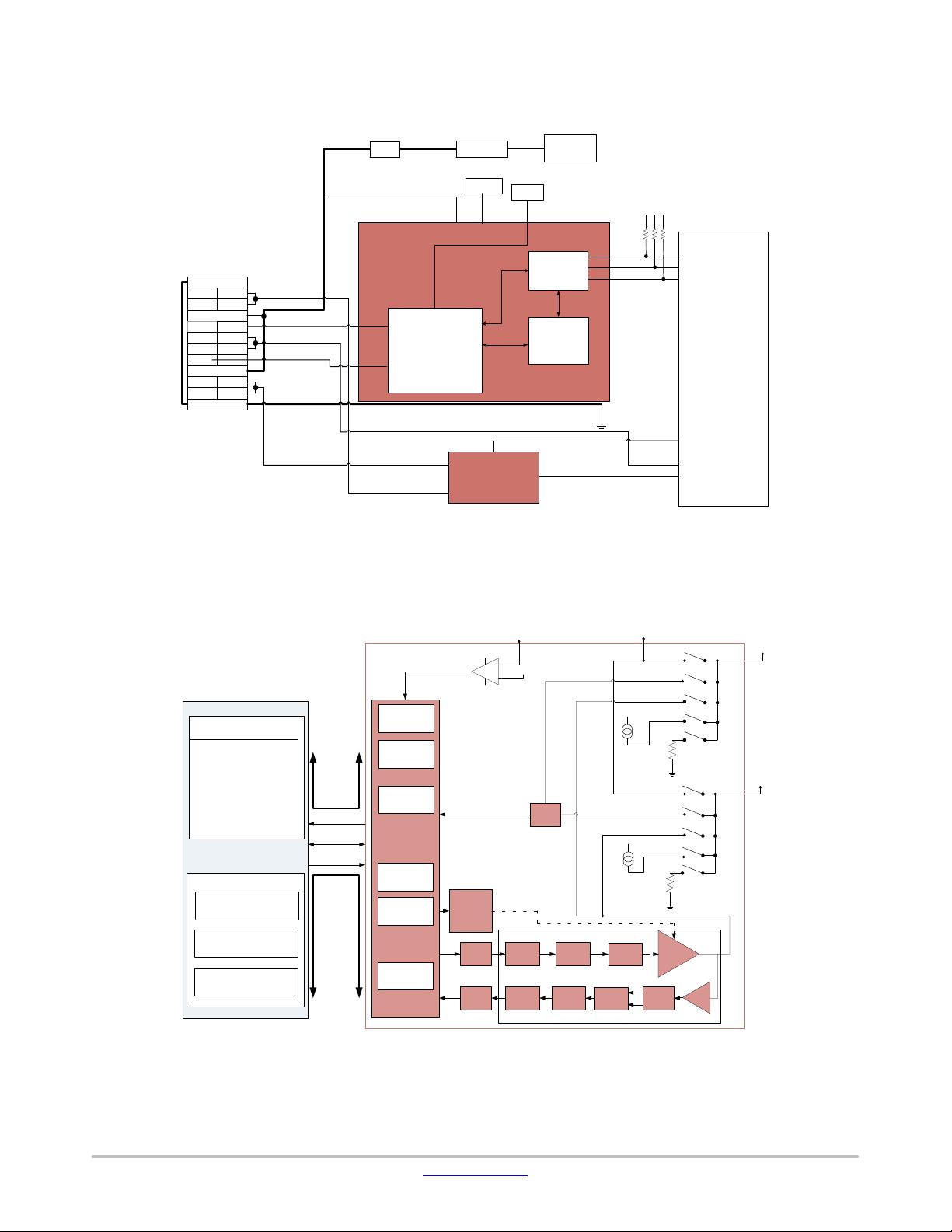
•完支持Type-C 1.2。成CC引"的功
♦机接/分离检测
♦机电流力指示
♦备电流力指示
♦#$%器&模式
♦'(&模式
♦动电)检测
•将CCx成到VCONN开,所有具有USB 3.1功的电源*
)提+流,制。
•USB电力(PD) 2.0,支持1.2版本
♦动GoodCRC报文响应
♦未收到GoodCRC时动-发报文
♦时,动--发报文
♦动硬-发命
•电池.尽支持(无电时支持SNK模式)
•功.!: I
CC
= 25 mA(典型)
•封0:
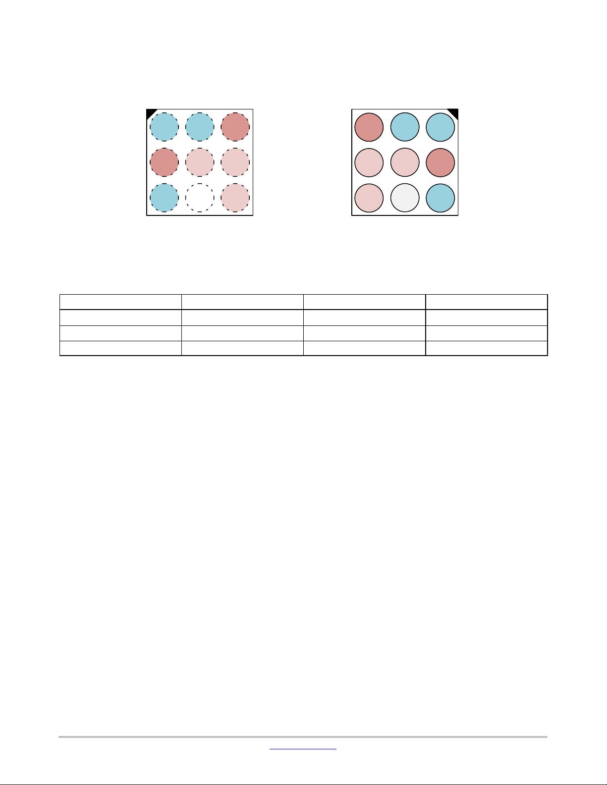
♦9焊点WLCSP (1.215 mm × 1.260 mm)
♦14引"MLP (2.5 mm × 2.5 mm, 0.5 mm12)
•智手机
•平板电3
•4型电3
•笔5本电3
•电源%器
•相机
•加密狗
www.onsemi.cn
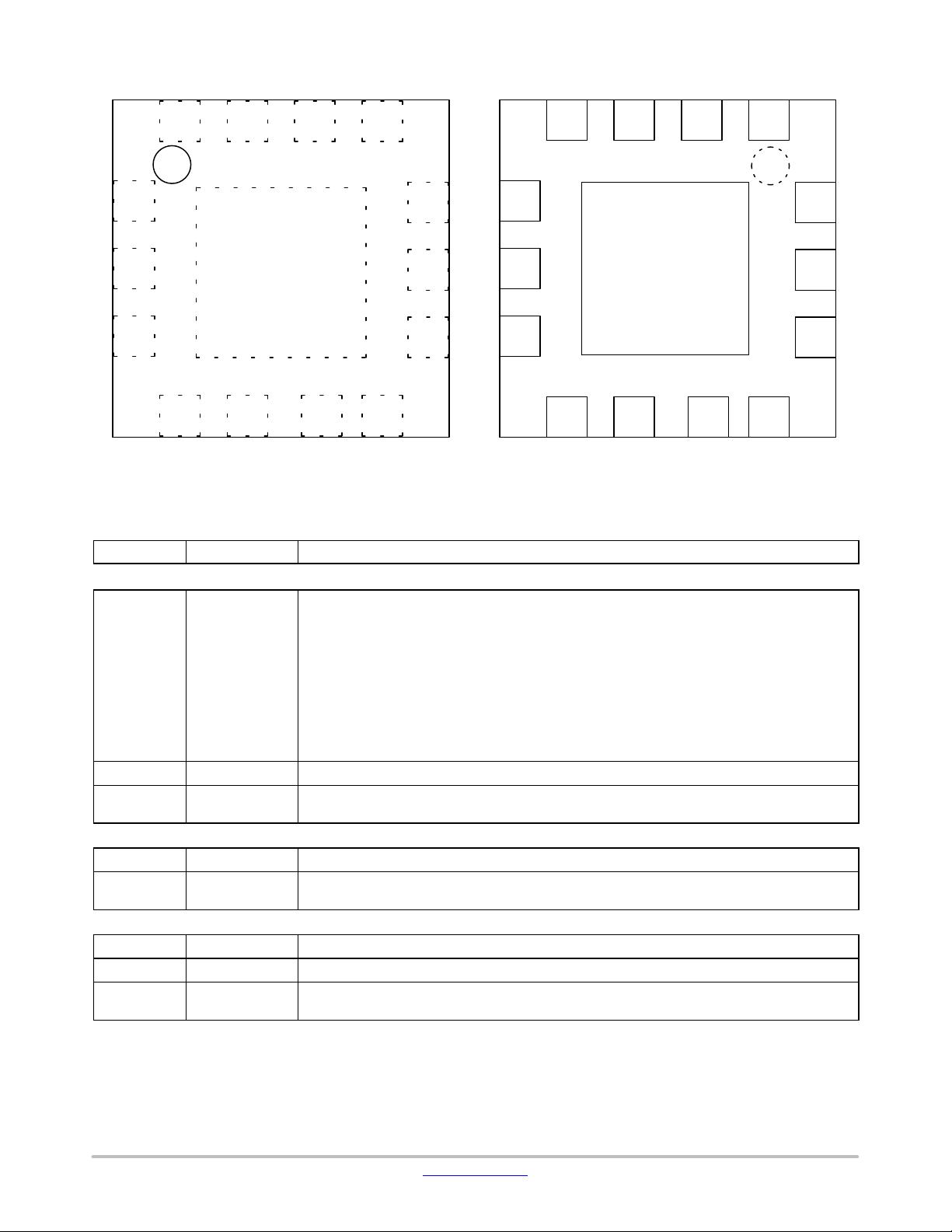
WLCSP9
CASE 567TN
See detailed ordering and shipping information on page 2 o
f
this data sheet.
ORDERING INFORMATION
WQFN14
CASE 510BR
剩余32页未读,继续阅读

weixin_44927660
- 粉丝: 2
- 资源: 7
 我的内容管理
收起
我的内容管理
收起
- 我的资源
快来上传第一个资源
 我的收益 登录查看自己的收益
 我的积分
登录查看自己的积分
我的积分
登录查看自己的积分
 我的C币
登录后查看C币余额
我的C币
登录后查看C币余额
 我的收藏
我的收藏  我的下载
我的下载  下载帮助
下载帮助

会员权益专享


最新资源
- c++校园超市商品信息管理系统课程设计说明书(含源代码) (2).pdf
- 建筑供配电系统相关课件.pptx
- 企业管理规章制度及管理模式.doc
- vb打开摄像头.doc
- 云计算-可信计算中认证协议改进方案.pdf
- [详细完整版]单片机编程4.ppt
- c语言常用算法.pdf
- c++经典程序代码大全.pdf
- 单片机数字时钟资料.doc
- 11项目管理前沿1.0.pptx
- 基于ssm的“魅力”繁峙宣传网站的设计与实现论文.doc
- 智慧交通综合解决方案.pptx
- 建筑防潮设计-PowerPointPresentati.pptx
- SPC统计过程控制程序.pptx
- SPC统计方法基础知识.pptx
- MW全能培训汽轮机调节保安系统PPT教学课件.pptx
资源上传下载、课程学习等过程中有任何疑问或建议,欢迎提出宝贵意见哦~我们会及时处理!
点击此处反馈


评论0