CMT2210/17AW
Rev 1.3 | Page 1/28
www.hoperf.com
CMT2210/17AW
Low-Cost 300 – 960 MHz OOK Stand-Alone RF Receiver
Copyright © By CMOSTEK
Features
Embedded EEPROM
Very Easy Development with RFPDK
All Features Programmable
Frequency Range
300 to 480 MHz (CMT2210AW)
300 to 960 MHz (CMT2217AW)
Symbol Rate: 0.1 to 40 ksps
Sensitivity: -113 dBm at 1 ksps, 0.1% BER
Configurable Receiver Bandwidth: 50 to 500 kHz
3-wire SPI Interface for EEPROM Programming
Stand-Alone, No External MCU Control Required
Configurable Duty-Cycle Operation Mode
Supply Voltage: 1.8 to 3.6 V
Low Power Consumption: 3.8 mA
Low Sleep Current
60 nA when Sleep Timer Off
440 nA when Sleep Timer On
RoHS Compliant
16-pin QFN 3x3 and SOP16 Package Options
Applications
Low-Cost Consumer Electronics Applications
Home and Building Automation
Infrared Receiver Replacements
Industrial Monitoring and Controls
Remote Automated Meter Reading
Remote Lighting Control System
Wireless Alarm and Security Systems
Remote Keyless Entry (RKE)
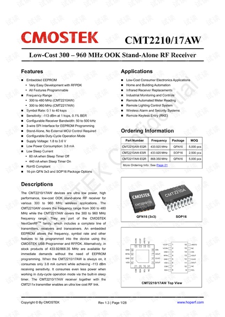
Ordering Information
Part Number Frequency Package MOQ
CMT2210AW-EQR 433.920 MHz QFN16 5,000 pcs
CMT2210AW-ESR 433.920 MHz SOP16 2,500 pcs
CMT2217AW-EQR 868.350 MHz QFN16 5,000 pcs
More Ordering Info: See Page 21
Descriptions
The CMT2210/17AW devices are ultra low power, high
performance, low-cost OOK stand-alone RF receiver for
various 300 to 960 MHz wireless applications. The
CMT2210AW covers the frequency range from 300 to 480
MHz while the CMT2217AW covers the 300 to 960 MHz
frequency range. They are part of the CMOSTEK
NextGenRF
TM
family, which includes a complete line of
transmitters, receivers and transceivers. An embedded
EEPROM allows the frequency, symbol rate and other
features to be programmed into the device using the
CMOSTEK USB Programmer and RFPDK. Alternatively, in
stock products of 433.92/868.35 MHz are available for
immediate demands without the need of EEPROM
programming. When the CMT2210/17AW is always on, it
consumes only 3.8 mA current while achieving -113 dBm
receiving sensitivity. It consumes even less power when
working in duty-cycle operation mode via the built-in sleep
timer. The CMT2210/17AW receiver together with the
CMT211x transmitter enables an ultra low cost RF link.
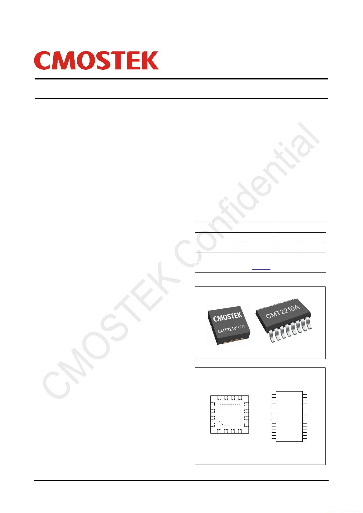
QFN16 (3X3) SOP16
GND
RFIN
GND
VDD
CSB
SDA
SCL
NC
XIN
XOUT
CLKO
DOUT
VCON
VCOP
nRSTO
NC
13
14
15
16
1 2 3 4
5
6
7
8
9101112
1
2
3
4
5
6
7
14
13
12
10
9
11
VCOP
VCON
GND
RFIN
GND
VDD
CSB
nRSTO
NC
XIN
XOUT
CLKO
DOUT
8
SDA
SCL
15
16
NC
CMT2210/17AW Top View


剩余27页未读,继续阅读

sam-zy
- 粉丝: 5260
- 资源: 55
 我的内容管理
收起
我的内容管理
收起
- 我的资源
快来上传第一个资源
 我的收益 登录查看自己的收益
 我的积分
登录查看自己的积分
我的积分
登录查看自己的积分
 我的C币
登录后查看C币余额
我的C币
登录后查看C币余额
 我的收藏
我的收藏  我的下载
我的下载  下载帮助
下载帮助

会员权益专享


最新资源
- zigbee-cluster-library-specification
- JSBSim Reference Manual
- c++校园超市商品信息管理系统课程设计说明书(含源代码) (2).pdf
- 建筑供配电系统相关课件.pptx
- 企业管理规章制度及管理模式.doc
- vb打开摄像头.doc
- 云计算-可信计算中认证协议改进方案.pdf
- [详细完整版]单片机编程4.ppt
- c语言常用算法.pdf
- c++经典程序代码大全.pdf
- 单片机数字时钟资料.doc
- 11项目管理前沿1.0.pptx
- 基于ssm的“魅力”繁峙宣传网站的设计与实现论文.doc
- 智慧交通综合解决方案.pptx
- 建筑防潮设计-PowerPointPresentati.pptx
- SPC统计过程控制程序.pptx
资源上传下载、课程学习等过程中有任何疑问或建议,欢迎提出宝贵意见哦~我们会及时处理!
点击此处反馈


评论0