OV7725:一款集成VGA摄像头与处理器的OmniVision传感器详解
需积分: 49 167 浏览量
更新于2023-05-11
收藏 1.07MB PDF 举报
本文档是OmniVision Technologies公司提供的OV7725摄像头芯片的详细资料,该芯片是一款专为VGA(640x480)分辨率设计的高性能CMOS图像传感器,集成了单芯片VGA相机和图像处理器的功能。OV7725的特点包括:
1. 低电压设计:作为一款低电压设备,它能够在保持高效能的同时,降低功耗,适合于电池供电的应用。
2. 多功能性:通过Serial Camera Control Bus (SCCB)接口,用户可以全面控制传感器,实现全帧、子采样或窗口模式下的8位或10位图像输出,支持多种图像格式。
3. 高速性能:最大支持60帧每秒的帧率,确保了实时视频捕获的能力。
4. 图像质量控制:内置丰富的图像处理功能,如曝光控制、伽马校正、白平衡调整、色彩饱和度和色相控制等,允许用户根据应用需求进行精细调节。
5. 集成度高:小巧的封装尺寸使得该芯片在有限的空间内提供了完整的影像解决方案,便于系统集成。
6. 技术与品牌:采用OmniPixel 2和OmniVision商标技术,体现了OmniVision Technologies公司在图像传感器领域的领先地位。
7. 文档状态:这是一份预发布数据手册,版本为1.1,可能随着技术更新而发生变化,用户需密切关注最新规格。
OV7725摄像头芯片是为满足高性能、灵活性和低功耗需求的理想选择,特别适用于那些对图像质量和处理速度有较高要求的应用,如手机摄像头、安防监控、工业自动化等领域。掌握并理解这些详细参数和功能,能够帮助工程师更好地设计和优化基于OV7725的系统方案。
Timing Specifications
Version 1.1, March 30, 2007 Proprietary to OmniVision Technologies, Inc. 7
O
mni ision
Timing Specifications
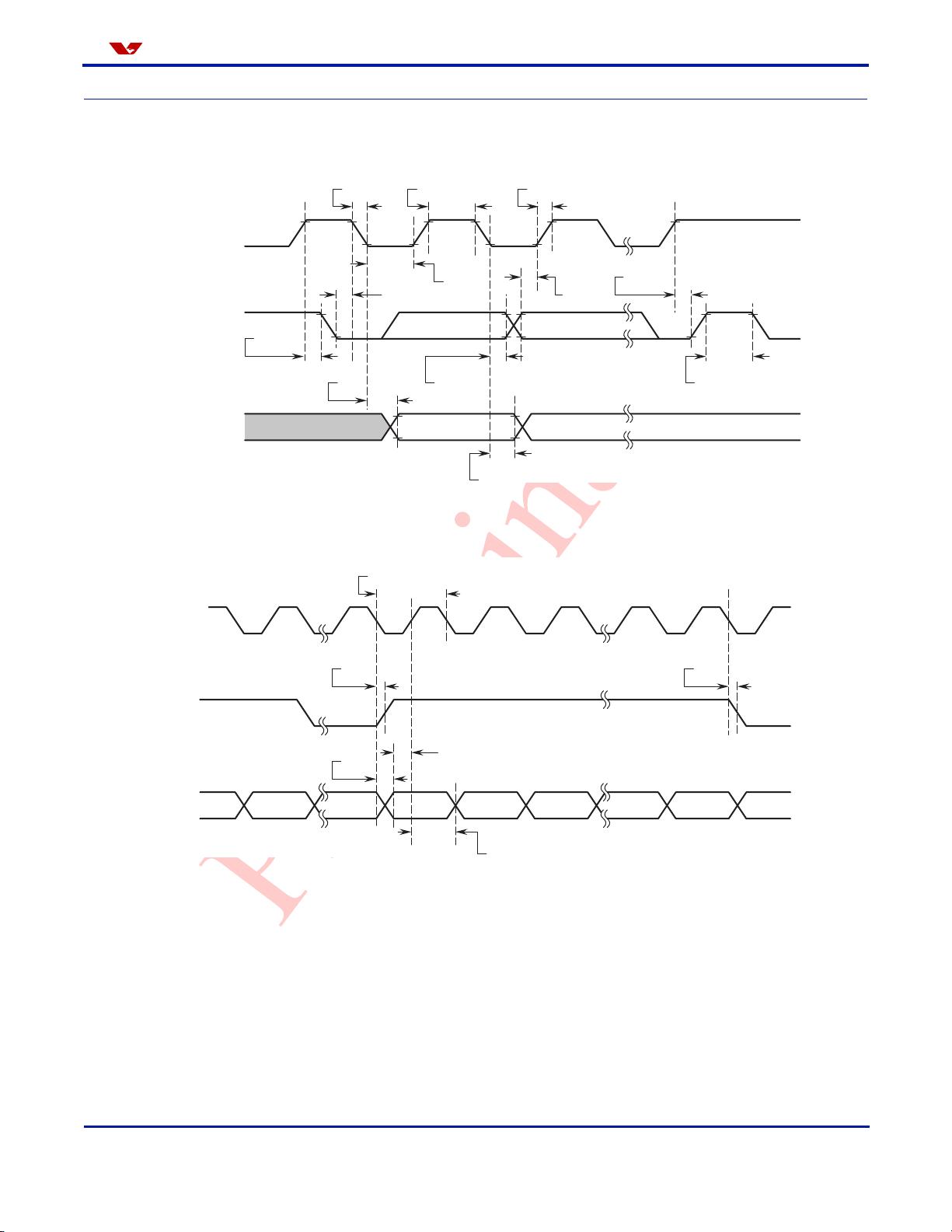
Figure 4 SCCB Timing Diagram
Figure 5 Horizontal Timing
SDA (OUT)
t
AA
t
DH
SCL
t
F
t
R
t
HIGH
t
LOW
t
SU:DAT
SDA (IN)
t
HD:DAT
t
SU:STO
t
SU:STA
t
HD:STA
t
BUF
7725CSP_DS_004
D[9:0]
HREF (row data)
last byte last bytezero first byte
PCLK
t
SU
t
HD
t
PCLK
t
PHL
t
PHL
t
PDV
7725CSP_DS_005
剩余35页未读,继续阅读
231 浏览量
171 浏览量
394 浏览量
231 浏览量
1653 浏览量
394 浏览量
388 浏览量
1174 浏览量
599 浏览量

huanghu1230
- 粉丝: 758
 我的内容管理
展开
我的内容管理
展开


最新资源
- ActiveMQ中Jms桥接实现的详解
- Hibernate开发必备:完整jar包及配置指南
- 精通C#设计模式:创建、结构与行为的综合指南
- 贪食蛇游戏源代码完整解析及jar包下载指南
- SHT10温湿度采集及LCD显示代码程序解析
- Java实现的FTP协议课程设计教程
- VC2010环境下非阻塞UDP通信实现教程
- 多普达系列手机刷入GSM程序指南
- destoon5.0实现产品图片扩容至10张教程
- Unity中使用NPOI库在.NET 4以上版本成功创建Word文档
- 多样化的加载动画:透明背景的loading.gif图标
- VISIO网页设计实用库:创意与效率并存
- C++编程速成教程TXT版完整内容解析
- QuickLook:Windows平台上的快速文件预览工具
- GitHub图像预览增强型Chrome扩展
- WPS 2019-2020校园版 VBA插件安装与宏功能开启指南