Analog Dialogue 40-02, February (2006) 1
ADC Input Noise: The Good,
The Bad, and The Ugly.
Is No Noise Good Noise?
By Walt Kester [walt.kester@analog.com]
INTRODUCTION
All analog-to-digital converters (ADCs) have a certain amount of
input-referred noise—modeled as a noise source connected in series
with the input of a noise-free ADC. Input-referred noise is not
to be confused with quantization noise, which is only of interest
when an ADC is processing time-varying signals. In most cases,
less input noise is better; however, there are some instances where
input noise can actually be helpful in achieving higher resolution.
If this doesn’t seem to make sense right now, read on to find out
how some noise can be good noise.
Input-Referred Noise (Code-Transition Noise)
Practical ADCs deviate from ideal ADCs in many ways. Input-
referred noise is certainly a departure from the ideal, and its
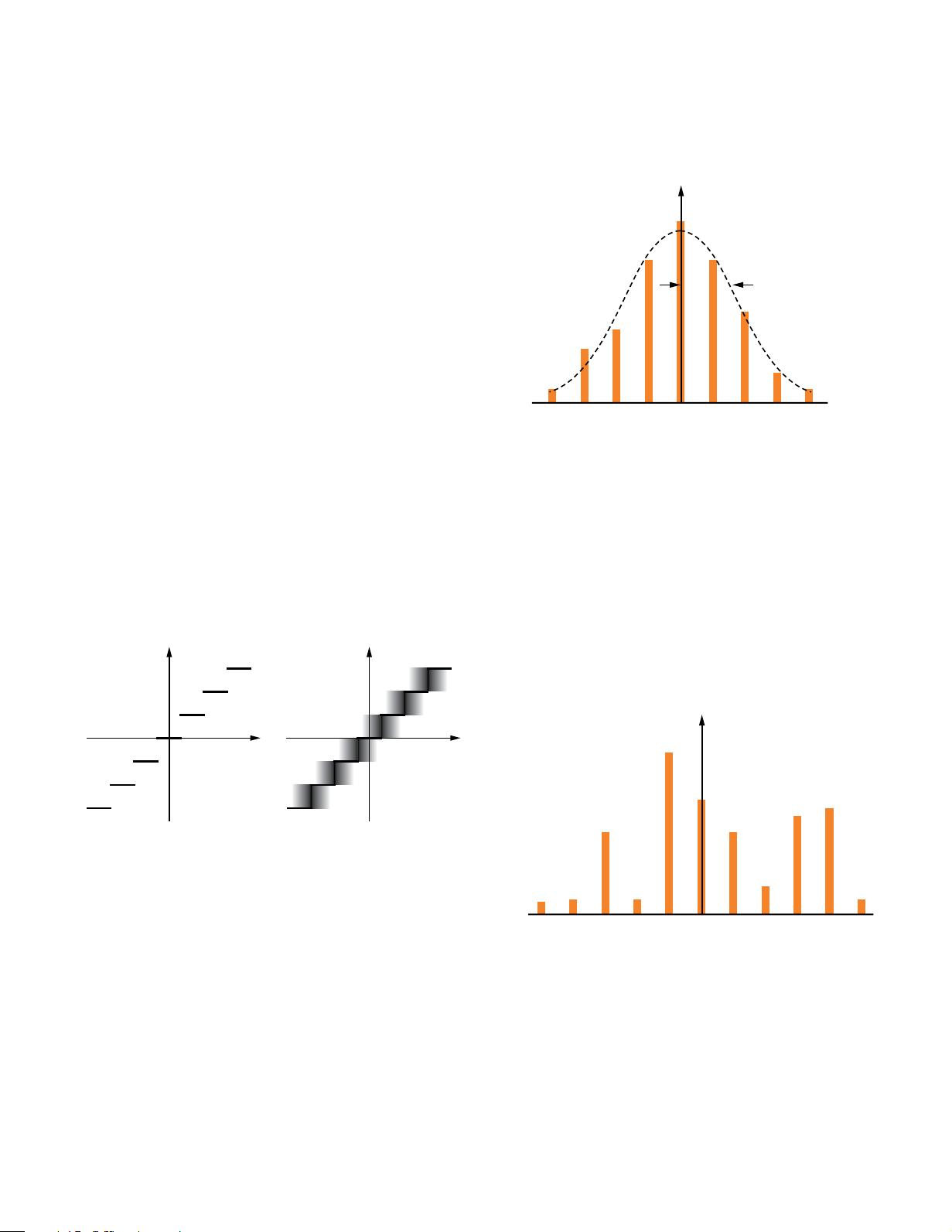
effect on the overall ADC transfer function is shown in Figure 1.
As the analog input voltage is increased, the “ideal” ADC (shown
in Figure 1a) maintains a constant output code until a transition
region is reached, at which point it instantly jumps to the next
value, remaining there until the next transition region is reached.
A theoretically perfect ADC has zero code-transition noise, and a
transition region width equal to zero. A practical ADC has a
certain amount of code transition noise, and therefore a finite
transition region width. Figure 1b shows a situation where
the width of the code transition noise is approximately one
least-significant bit (LSB) peak-to-peak.
ANALOG
INPUT
DIGITAL
OUTPUT
(a) IDEAL ADC
ANALOG
INPUT
DIGITAL
OUTPUT
(b) ACTUAL ADC
Figure 1. Code-transition noise (input-referred noise)
and its effect on ADC transfer function.
Internally, all ADC circuits produce a certain amount of rms noise
due to resistor noise and “kT/C” noise. This noise, present even
for dc input signals, accounts for the code-transition noise, now
generally referred to as input-referred noise. Input-referred noise is
most often characterized by examining the histogram of a number
of output samples, while the input to the ADC is held constant at a
dc value. The output of most high speed or high resolution ADCs
is a distribution of codes, typically centered around the nominal
value of the dc input (see Figure 2).
To measure the amount of input-referred noise, the input of the
ADC is either grounded or connected to a heavily decoupled
voltage source, and a large number of output samples are
collected and plotted as a histogram (referred to as a grounded-
input histogram if the input is nominally at zero volts). Since the
noise is approximately Gaussian, the standard deviation of the
histogram, , which can be calculated, corresponds to the effective
http://www.analog.com/analogdialogue
input rms noise. See Further Reading 6 for a detailed description
of how to calculate the value of from the histogram data. It is
common practice to express this rms noise in terms of LSBs
rms, corresponding to an rms voltage referenced to the ADC
full-scale input range. If the analog input range is expressed as
digital numbers, or counts, input values, such as , can be expressed
as a count of the number of LSBs.
NUMBER OF
OCCURRENCES
STANDARD DEVIATION
= RMS NOISE (LSBs)
P-P INPUT NOISE
� 6.6 � RMS NOISE
n – 4 n – 3 n – 2 n – 1 n
OUTPUT CODE
n + 1 n + 2 n + 3 n + 4
Figure 2. Effect of input-referred noise on ADC grounded-
input histogram for an ADC with a small amount of DNL.
Although the inherent differential nonlinearity (DNL) of the ADC
will cause deviations from an ideal Gaussian distribution (for
instance, some DNL is evident in Figure 2), it should be at least
approximately Gaussian. If there is significant DNL, the value
of should be calculated for several different dc input voltages
and the results averaged. If the code distribution is significantly
non-Gaussian, as exemplified by large and distinct peaks and
valleys, for instance—this could indicate either a poorly designed
ADC or—more likely—a bad PC board layout, poor grounding
techniques, or improper power supply decoupling (see Figure 3).
Another indication of trouble is when the width of the distribution
changes drastically as the dc input is swept over the ADC input
voltage range.
NUMBER OF
OCCURRENCES
n – 5 n – 4 n – 3 n – 2 n – 1 n
OUTPUT CODE
n + 1 n + 2 n + 3 n + 4 n + 5
Figure 3. Grounded-input histogram for poorly designed
ADC and/or poor layout, grounding, or decoupling.
Noise-Free (Flicker-Free) Code Resolution
The noise-free code resolution of an ADC is the number of bits
of resolution beyond which it is impossible to distinctly resolve
individual codes. This limitation is due to the effective input noise
(or input-referred noise) associated with all ADCs and described
above, usually expressed as an rms quantity with the units of
LSBs rms. Multiplying by a factor of 6.6 converts the rms noise into
a useful measure of peak-to-peak noise—the actual uncertainty with
which a code can be identified—expressed in LSBs peak-to-peak.


