
Charge
Pump
Vtune
CPout
RFoutAP
Sigma-Delta
Modulator
N Divider
OSCin
Douber
Post-R
Divider
Multiplier
Pre-R
Divider
ϕ
Vcc
RFoutAM
RFoutBP
Vcc
Channel
Divider
Loop Filter
Phase
Detector
Serial Interface
Control
SDI
SCK
CSB
MUXout
OSCinP
OSCinM
Input
signal
RFoutBM
MUX
MUX
SYSREF
Copyright © 2017, Texas Instruments Incorporated
Product
Folder
Order
Now
Technical
Documents
Tools &
Software
Support &
Community
An IMPORTANT NOTICE at the end of this data sheet addresses availability, warranty, changes, use in safety-critical applications,
intellectual property matters and other important disclaimers. PRODUCTION DATA.
LMX2594
SNAS696C –MARCH 2017–REVISED APRIL 2019
LMX2594 15-GHz Wideband PLLATINUM™ RF Synthesizer
With Phase Synchronization and JESD204B Support
1
1 Features
1
• 10-MHz to 15-GHz output frequency
• –110 dBc/Hz phase noise at 100-kHz offset with
15-GHz carrier
• 45-fs rms jitter at 7.5 GHz (100 Hz to 100 MHz)
• Programmable output power
• PLL key specifications
– Figure of merit: –236 dBc/Hz
– Normalized 1/f noise: –129 dBc/Hz
– High phase detector frequency
– 400-MHz integer mode
– 300-MHz fractional mode
– 32-bit fractional-N divider
• Remove integer boundary spurs with
programmable input multiplier
• Synchronization of output phase across multiple
devices
• Support for SYSREF with 9-ps resolution
programmable delay
• Frequency ramp and chirp generation ability for
FMCW applications
• < 20-µs VCO calibration speed
• 3.3-V single power supply operation
2 Applications
• 5G and mm-Wave wireless infrastructure
• Test and measurement equipment
• Radar
• MIMO
• Phased array antennas and beam forming
• High-speed data converter clocking (supports
JESD204B)
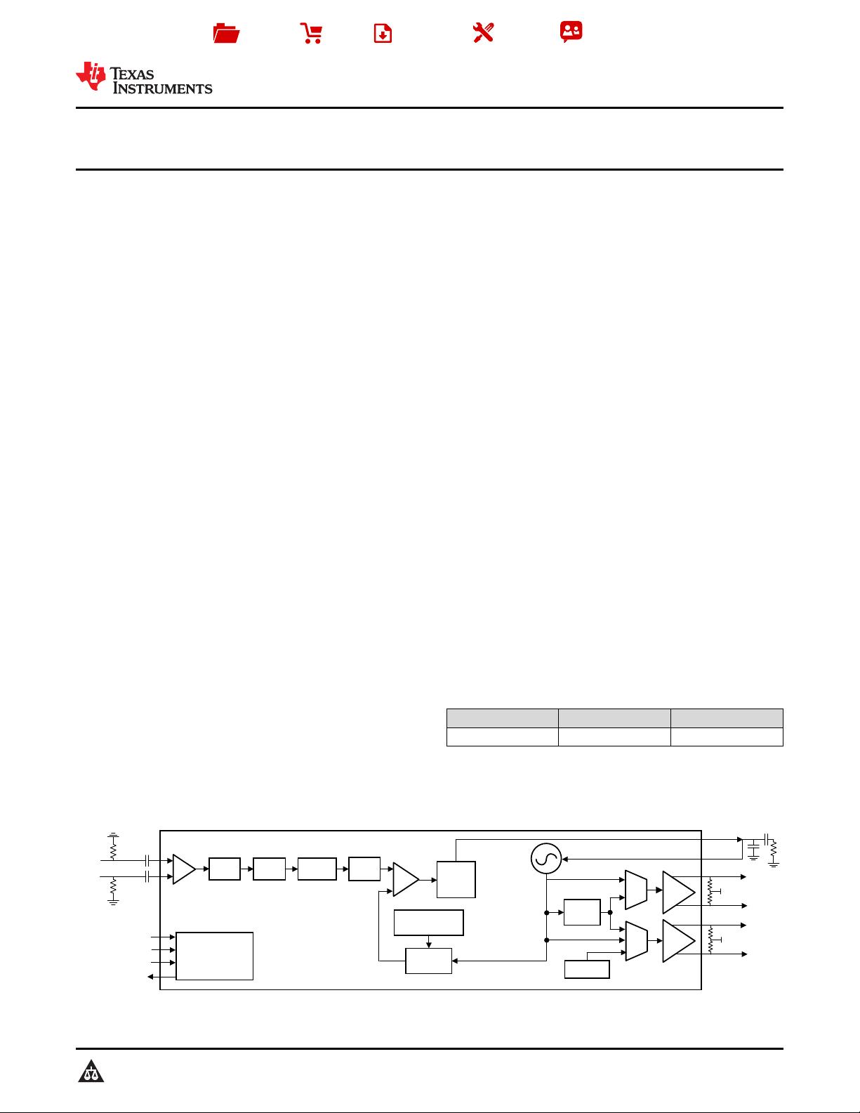
3 Description
The LMX2594 is a high-performance, wideband
synthesizer that can generate any frequency from 10
MHz to 15 GHz without using an internal doubler,
thus eliminating the need for sub-harmonic filters. The
high-performance PLL with figure of merit of –236
dBc/Hz and high-phase detector frequency can attain
very low in-band noise and integrated jitter. The high-
speed N-divider has no pre-divider, thus significantly
reducing the amplitude and number of spurs. There is
also a programmable input multiplier to mitigate
integer boundary spurs.
The LMX2594 allows users to synchronize the output
of multiple devices and also enables applications that
need deterministic delay between input and output. A
frequency ramp generator can synthesize up to two
segments of ramp in an automatic ramp generation
option or a manual option for maximum flexibility. The
fast calibration algorithm allows changing frequencies
faster than 20 µs. The LMX2594 adds support for
generating or repeating SYSREF (compliant to
JESD204B standard) designed for low-noise clock
sources in high-speed data converters. A fine delay
adjustment (9-ps resolution) is provided in this
configuration to account for delay differences of board
traces.
The output drivers within LMX2594 deliver output
power as high as 7 dBm at 15-GHz carrier frequency.
The device runs from a single 3.3-V supply and has
integrated LDOs that eliminate the need for on-board
low noise LDOs.
Device Information
(1)
PART NUMBER PACKAGE BODY SIZE (NOM)
LMX2594 VQFN (40) 6.00 mm × 6.00 mm
(1) For all available packages, see the orderable addendum at
the end of the data sheet.
Simplified Schematic


剩余75页未读,继续阅读

zhaoyixin2016
- 粉丝: 1
- 资源: 2
 我的内容管理
收起
我的内容管理
收起
- 我的资源
快来上传第一个资源
 我的收益 登录查看自己的收益
 我的积分
登录查看自己的积分
我的积分
登录查看自己的积分
 我的C币
登录后查看C币余额
我的C币
登录后查看C币余额
 我的收藏
我的收藏  我的下载
我的下载  下载帮助
下载帮助

会员权益专享


最新资源
- 基于单片机的瓦斯监控系统硬件设计.doc
- 基于单片机的流量检测系统的设计_机电一体化毕业设计.doc
- 基于单片机的继电器设计.doc
- 基于单片机的湿度计设计.doc
- 基于单片机的流量控制系统设计.doc
- 基于单片机的火灾自动报警系统毕业设计.docx
- 基于单片机的铁路道口报警系统设计毕业设计.doc
- 基于单片机的铁路道口报警研究与设计.doc
- 基于单片机的流水灯设计.doc
- 基于单片机的时钟系统设计.doc
- 基于单片机的录音器的设计.doc
- 基于单片机的万能铣床设计设计.doc
- 基于单片机的简易安防声光报警器设计.doc
- 基于单片机的脉搏测量器设计.doc
- 基于单片机的家用防盗报警系统设计.doc
- 基于单片机的简易电子钟设计.doc
资源上传下载、课程学习等过程中有任何疑问或建议,欢迎提出宝贵意见哦~我们会及时处理!
点击此处反馈


