没有合适的资源?快使用搜索试试~ 我知道了~
首页mini-lvds.pdf
资源详情
资源评论
资源推荐

mini-LVDS Specification
Version 0.1
2001 Texas Instruments Page 1 of 22
Confidential
Mini-LVDS Interface Specification
Revision 0.1
This is a draft standard and is subject to change. Systems built to this draft standard may not be
compliant with the standard when it is published in its final form.

mini-LVDS Specification
Version 0.1
2001 Texas Instruments Page 2 of 22
Confidential
1.0 Introduction
The trend towards higher and higher resolutions in flat panel displays, particularly LCD panels, is
pushing the capabilities of conventional interfaces towards display drivers to the limit. The aggregate
bandwidth requirement for state-of-the-art displays (e.g. UXGA and QXGA) is already in the range of
5 Mbps, and will increase in the near future. This necessitates a large number of connections between
the timing controller and the display drivers, with the result that the interconnect becomes the
bottleneck in further reduction of display size. EMI generation by this wide interconnect is another
problem. The conventional parallel CMOS interface which has served well for low resolution displays
in the past is no longer a viable solution for today’s displays.
mini-LVDS is a high speed serial interface that solves these problems. This specification describes the
electrical and logical specifications of this interface. mini-LVDS offers a low EMI, high bandwidth
interface towards display drivers, which is particularly well suited for TFT LCD panel column drivers.
A TFT LCD panel is a two-dimensional array of pixels, arranged in n rows of m columns. Each pixel
consists of 3 adjacent sub-pixels (one each for Red, Green and Blue) in the same row. The panel is
written into using an active matrix addressing scheme, whereby an entire row of pixels is updated
simultaneously by column drivers. The rows are updated sequentially from the first row to the last,
after which the process repeats. The timing controller has to source video data for the entire row of
pixels in one line duration (~ 10 us). This video data consists of 6 (or 8) bits of intensity information
for each sub-pixel.
The timing controller typically gets video data from a graphics controller. The incoming video data has
format control information to delimit video frames and lines. The timing controller extracts the video
data and redistributes it to the column drivers, at the same time generating control signals for the row
drivers for addressing the TFT matrix.

mini-LVDS Specification
Version 0.1
2001 Texas Instruments Page 3 of 22
Confidential
2.0 Scope
mini-LVDS is the interface between the timing controller and the column drivers (Figure 2.1). It is
described in subsequent sections of this document.
Note that the standard does not cover the signals between the timing controller and the row drivers, or
the signals between the column drivers (which may be used, for example, to put column drivers into
power-down mode).
Column Drivers
Row Drivers
Row 1
Row 2
Row n
Column 1 Column 2 Column m
Timing
Controller
mini-LVDS
Input video
Figure 2.1

mini-LVDS Specification
Version 0.1
2001 Texas Instruments Page 4 of 22
Confidential
3.0 Overview
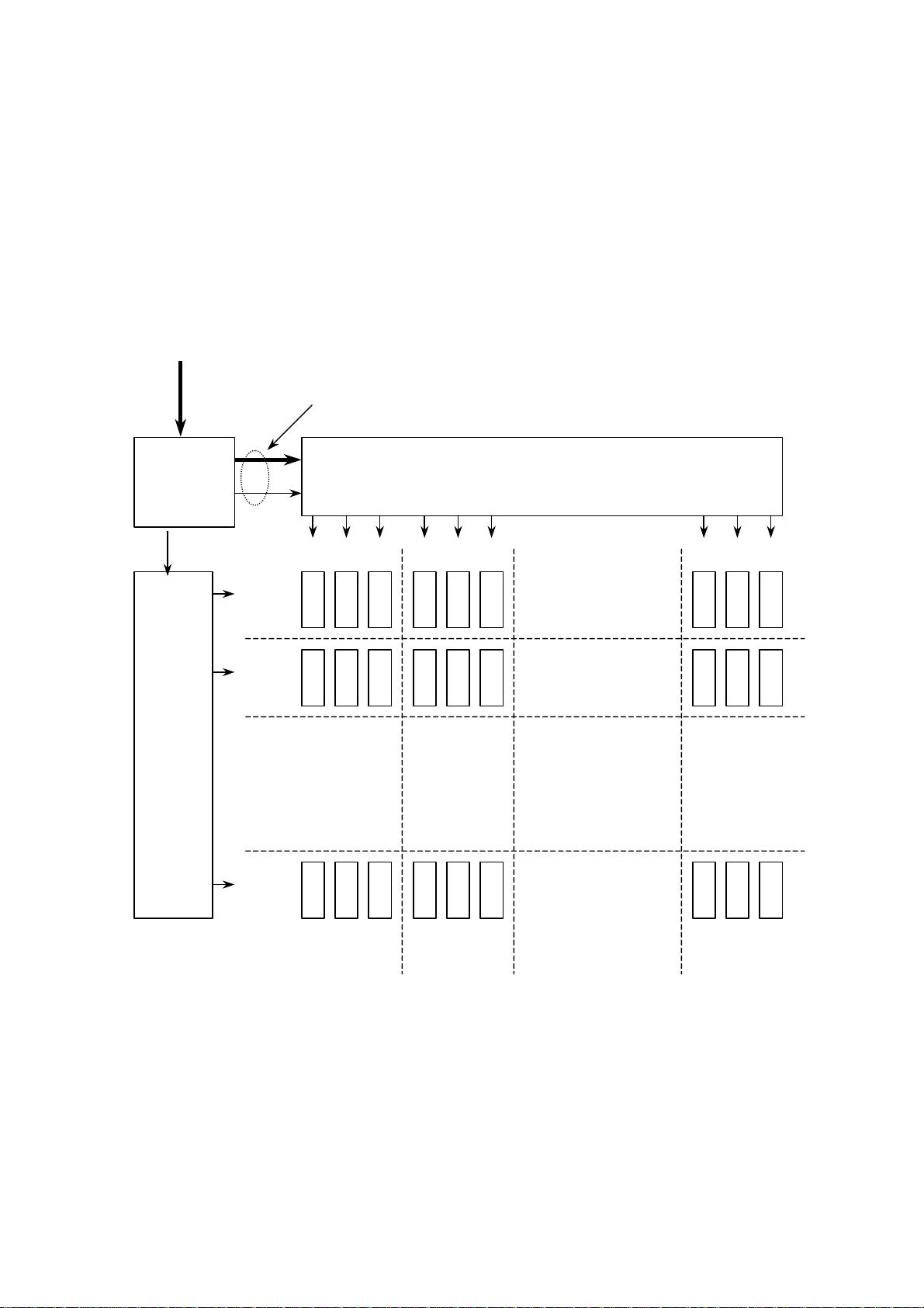
Mini-LVDS is a uni-directional interface from the timing controller to the column drivers.
Topologically, it is a dual bus, with the buses carrying video data for the left and the right halves of the
panel, respectively. These buses are subsequently referred to as RLV and LLV for the right half and the
left half respectively. (Figure 3.1)
Physically, each bus consists of a number of pairs of transmission lines on a printed circuit board, with
each pair carrying differential serialized video and control information. The number of signal pairs is
left to implementation, and will be determined primarily by the maximum frequency that the column
driver semiconductor technology can support. The individual pairs making up XLV (X is either R or L)
are called XLVi, with ‘i’ ranging from 0 to n for a bus consisting of n+1 data pairs. The two lines
constituting the pair XLVi are XLViP and XLViM with the P and M designating the positive and the
negative lines of the pair. XLVi is deemed to be at a logic HIGH (logic state = 1) if the voltage on
XLViP is more than the voltage on XLViM.
RLV and LLV each also include clocks, which, like data signals, are differential pairs. To minimize
EMI without increasing receiver complexity drastically, data transfer occurs on both rising and falling
edges of the clock, i.e. the clock frequency is half of the maximum data transfer rate. The clock pairs
will be referred to as XLVCLK (X is either R or L), and the individual lines making up the pair will be
referred to as XLVCLKP and XLVCLKM. (Figure 3.2)
In addition to the differential pairs carrying video data, there are two more signals (TP1 and POL) that
make up mini-LVDS. These are CMOS level rail-to rail signals shared by both RLV and LLV. TP1 is
essentially a line delimiter, generated by the timing controller to signal end of data transfer every line.
POL controls the polarity of the driver outputs.

mini-LVDS Specification
Version 0.1
2001 Texas Instruments Page 5 of 22
Confidential
XLV0P
XLV0M
XLViP
XLViM
XLVnP
XLVnM
XLVCLKP
XLVCLKM
XLV0
XLVi
XLVn
XLVCLK
TP1
POL
XLV
mini-LVDS
RLV
LLV
TP1, POL
Timing
Controller
Source (Column) Drivers
Figure 3.1
Figure 3.2
剩余21页未读,继续阅读


安全验证
文档复制为VIP权益,开通VIP直接复制

评论0