
1. General description
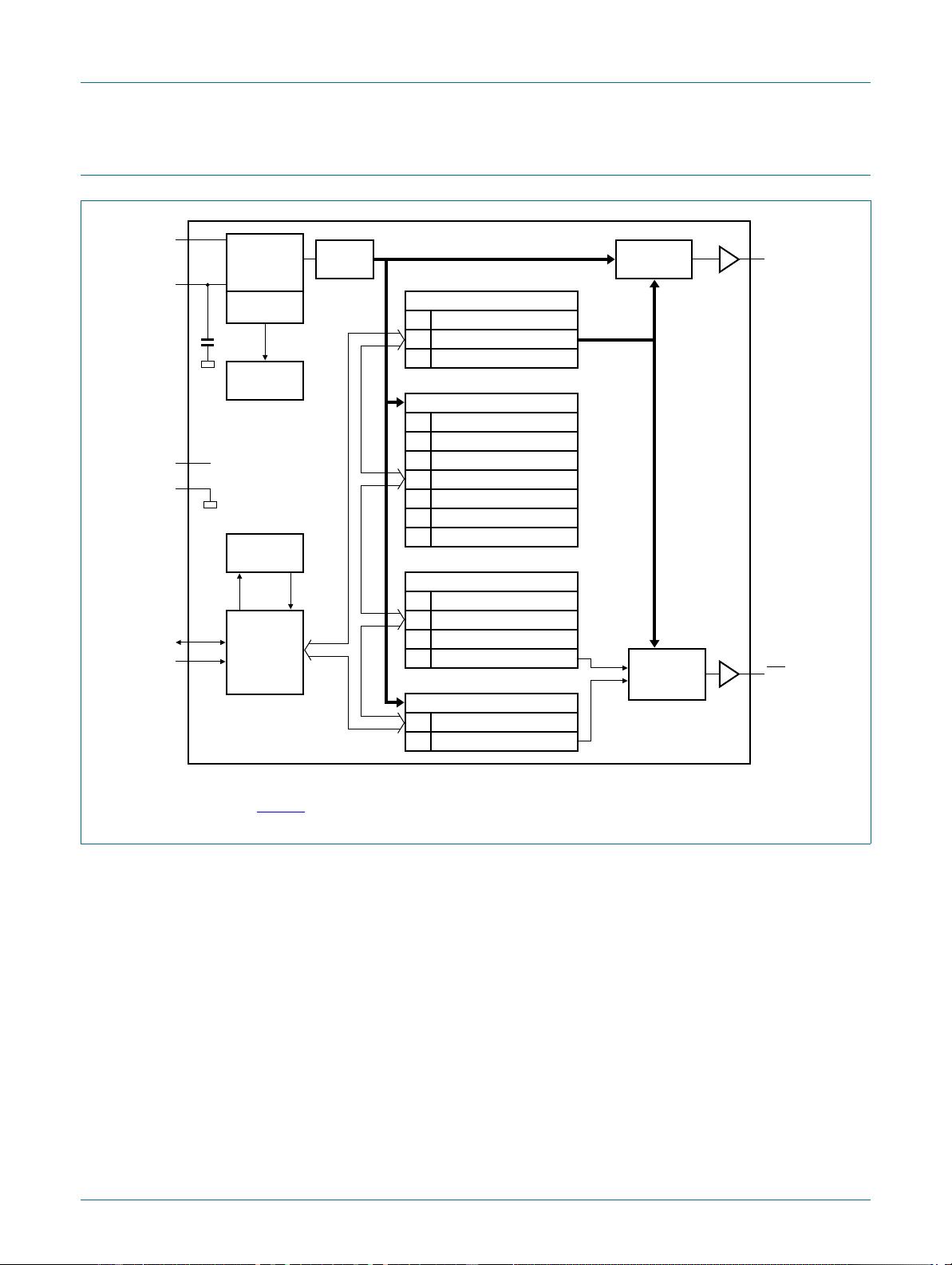
The PCF8563 is a CMOS
1
Real-Time Clock (RTC) and calendar optimized for low power
consumption. A programmable clock output, interrupt output, and voltage-low detector are
also provided. All addresses and data are transferred serially via a two-line bidirectional
I
2
C-bus. Maximum bus speed is 400 kbit/s. The register address is incremented
automatically after each written or read data byte.
2. Features and benefits
Provides year, month, day, weekday, hours, minutes, and seconds based on a
32.768 kHz quartz crystal
Century flag
Clock operating voltage: 1.0 V to 5.5 V at room temperature
Low backup current; typical 0.25 Aat V
DD
= 3.0 V and T
amb
=25C
400 kHz two-wire I
2
C-bus interface (at V
DD
= 1.8 V to 5.5 V)
Programmable clock output for peripheral devices (32.768 kHz, 1.024 kHz, 32 Hz, and
1Hz)
Alarm and timer functions
Integrated oscillator capacitor
Internal Power-On Reset (POR)
I
2
C-bus slave address: read A3h and write A2h
Open-drain interrupt pin
3. Applications
Mobile telephones
Portable instruments
Electronic metering
Battery powered products
PCF8563
Real-time clock/calendar
Rev. 10 — 3 April 2012 Product data sheet
1. The definition of the abbreviations and acronyms used in this data sheet can be found in Section 18.

剩余49页未读,继续阅读

barehua82
- 粉丝: 0
- 资源: 6
 我的内容管理
收起
我的内容管理
收起
- 我的资源
快来上传第一个资源
 我的收益 登录查看自己的收益
 我的积分
登录查看自己的积分
我的积分
登录查看自己的积分
 我的C币
登录后查看C币余额
我的C币
登录后查看C币余额
 我的收藏
我的收藏  我的下载
我的下载  下载帮助
下载帮助

会员权益专享


最新资源
- zigbee-cluster-library-specification
- JSBSim Reference Manual
- c++校园超市商品信息管理系统课程设计说明书(含源代码) (2).pdf
- 建筑供配电系统相关课件.pptx
- 企业管理规章制度及管理模式.doc
- vb打开摄像头.doc
- 云计算-可信计算中认证协议改进方案.pdf
- [详细完整版]单片机编程4.ppt
- c语言常用算法.pdf
- c++经典程序代码大全.pdf
- 单片机数字时钟资料.doc
- 11项目管理前沿1.0.pptx
- 基于ssm的“魅力”繁峙宣传网站的设计与实现论文.doc
- 智慧交通综合解决方案.pptx
- 建筑防潮设计-PowerPointPresentati.pptx
- SPC统计过程控制程序.pptx
资源上传下载、课程学习等过程中有任何疑问或建议,欢迎提出宝贵意见哦~我们会及时处理!
点击此处反馈


评论0