没有合适的资源?快使用搜索试试~ 我知道了~
首页模拟工程师电路设计指导手册_数据转换
资源详情
资源评论
资源推荐

Analog Engineer’s
Circuit Cookbook: Data Converters
IN
VREF
GND
V
DAC
DAC
Vin
5.0 V 3.0 V
AVDD DVDD
GND

Analog Engineer’s Circuit Cookbook:
Data Converters
Second Edition
SLYY138 - 03/2019
Special thanks for technical contribution:
Manuel Chavez
Luis Chioye
Kevin Duke
Aaron Estrada
Paul Frost
Abhijeet Godbole
Reed Kaczmarek
Art Kay
Dale Li
Peggy Liska
Bryan McKay
Garrett Sattereld
Uttama Kumar Satu
Evan Sawyer
Alex Smith
Cynthia Sosa
Collin Wells

Analog Engineer’s
Circuit Cookbook: Data Converters
(Second Edition)
Message from the editors:
The Analog Engineer’s Circuit Cookbook: Data Converters provides analog-to-digital converter (ADC) and digital-to-analog converter
(DAC) sub-circuit ideas that can be quickly adapted to meet your specific system needs. Each circuit is presented as a “definition-by-
example.” They include step-by-step instructions, like a recipe, with formulas enabling you to adapt the circuit to meet your design
goals. Additionally, all circuits are verified with SPICE simulations and include links to the corresponding TINA-TI
TM
SPICE circuits.
We’ve provided at least one recommended data converter for each circuit, but you can swap it with another device if you’ve found one
that’s a better fit for your design. You can search our large portfolio of data converters at www.ti.com/DC.
Our circuits require a basic understanding of amplifier and data converter concepts. If you’re new to data converter design, we highly
recommend completing our TI Precision Labs (TIPL) training series. TIPL includes courses on introductory topics, such as device
architecture, as well as advanced, application-specific problem-solving, using both theory and practical knowledge. Check out our
curriculum for Amplifiers, Data Converters and more at: www.ti.com/precisionlabs.
We plan to update this e-book with new ADC and DAC circuit building blocks and encourage you to see if your version is the latest at
www.ti.com/circuitcookbooks. If you have feedback on any of our existing circuits or would like to request additional data converter
circuits for the next edition of this e-book, please contact us at adccookbook@list.ti.com.
We hope you find our collection of data converter circuits helpful in developing your designs!
Additional resources to explore
TI Precision Labs
ti.com/precisionlabs
• On-demand courses and tutorials ranging from introductory to
advanced concepts that focus on application-specific problem solving
• Hands-on labs and evaluation modules (EVM) available
- TIPL Op Amps experimentation platform, ti.com/TIPL-amp-evm
- TIPL SAR ADC experimentation platform, ti.com/TIPL-adc-evm
Analog Engineer’s Pocket Reference
ti.com/analogrefguide
• PCB, analog and mixed-signal design formulae; includes conversions,
tables and equations
• e-book, iTunes and Android apps and hardcopy available
The Signal e-book
ti.com/signalbook
• Short, bite-sized lessons on on op-amp design topics, such as offset
voltage, input bias current, stability, noise and more
Analog Wire Blog
ti.com/analogwire
• Technical blogs written by analog experts that include tips, tricks and
design techniques
TI Designs
ti.com/tidesigns
• Ready-to-use reference designs with theory, calculations,
simulations schematics, PCB files and bench test results
Data Converter Parametric Quick Search
• Find your next precision or high-speed ADC, ti.com/ADC-search
• Find your next precision or high-speed DAC, ti.com/DAC-search
DIY Amplifier Circuit Evaluation Module (DIYAMP-EVM)
ti.com/DIYAMP-EVM
• Single-channel circuit evaluation module providing SC70, SOT23
and SOIC package options in 12 popular amplifier configurations
Dual-Channel DIY Amplifier Circuit Evaluation Module
(DUAL-DIYAMP-EVM)
ti.com/dual-diyamp-evm
• Dual-channel circuit evaluation module in an SOIC-8 package with
10 popular amplifier configurations
TINA-TI simulation software
ti.com/tool/tina-ti
• Complete SPICE simulator for DC, AC, transient and noise analysis
• Includes schematic entry and post-processor for waveform math
Analog Engineer’s Calculator
ti.com/analogcalc
• ADC and amplifier design tools, noise and stability analysis,
PCB and sensor tools
TI E2E
™
Community
ti.com/e2e
• Support forums for all TI products
The platform bar is a trademark of Texas Instruments.
©2019 Texas Instruments Incorporated.
Analog Engineer’s
Circuit Cookbook: Data Converters
IN
VREF
GND
V
DAC
DAC
Vin
5.0V 3.0V
AVDD DVDD
GND
Analog Engineer’s
Circuit Cookbook: Amplifiers
Want more circuits?
• Download the Analog Engineer’s
Circuit Cookbook for amplifiers
• Browse a complete list of amplifier
and data converter circuits
Visit ti.com/circuitcookbooks

Analog-to-digital converter (ADC)
Low-Power/Cost-Optimized Circuits
Driving a SAR ADC directly without a front-end buffer circuit (low-power,
low-sampling-speed DAQ) ..........................................................................5
Low-power sensor measurements: 3.3-V, 1-ksps, 12-bit, single-ended,
dual-supply circuit ....................................................................................10
Low-power sensor measurements: 3.3-V, 1-ksps, 12-bit, single-ended,
Level Translation Input Drive Circuits
Circuit for driving a high-voltage SAR with an instrumentation amplifier
....23
Circuit for driving high-voltage SAR ADC with a buffered instrumentation
amplifier .....................................................................................................29
Circuit for driving high-voltage SAR ADCs for high-voltage, true differential
signal acquisition ......................................................................................36
Circuit to increase input range on an integrated analog front end (AFE)
SAR ADC ...................................................................................................45
High common-mode differential input voltage to ±10-V ADC input circuit
...... 50
High-current battery monitor circuit: 0−10 A, 0−10 kHz, 18 bit ...............57
High-input impedance, true differential, analog front end (AFE) attenuator
circuit for SAR ADCs .................................................................................63
High-voltage battery monitor circuit: ±20 V, 0-10 kHz, 18-bit fully
differential .................................................................................................. 71
Single-ended to differential signal conversion using an op amp and FDA
for unipolar signals ................................................................................... 78
Single-ended-to-differential circuit using an op amp and fully-differential
amplifier (FDA) for bipolar signals..............................................................85
Single-ended to differential using a two op-amp circuit ..........................92
True differential, 4 × 2 MUX, analog front end, simultaneous-sampling
ADC circuit ...............................................................................................100
Low-Level Sensor Input Circuits
Circuit for driving a switched-capacitor SAR ADC with a buffered
instrumentation amplifier ......................................................................109
Circuit for driving a switched-capacitor SAR ADC with an
instrumentation amplifier ......................................................................117
Circuit for driving an ADC with an instrumentation amplifier in high gain
..124
Low-input bias-current front end SAR ADC circuit ..............................131
High-side current shunt monitor circuit to 3-V single-ended ADC .......136
Two-wire PT100 RTD measurement circuit with low-side reference ....142
Three-wire PT100 RTD measurement circuit with high-side reference
and two IDAC current sources .............................................................148
Three-wire PT100 RTD measurement circuit with low-side reference
and one IDAC current source ...............................................................155
Three-wire PT100 RTD measurement circuit with low-side reference
and two IDAC current sources .............................................................161
Four-wire PT100 RTD measurement circuit with low-side reference ...168
Two-channel, K-type thermocouple measurement circuit with internal
temperature sensor CJC ......................................................................174
Input Protection, Filtering and Isolation Circuits
±12-V voltage sensing circuit with an isolated amplier and pseudo-
differential input SAR ADC ...................................................................181
±12-V voltage sensing circuit with an isolated amplier and differential
input SAR ADC .....................................................................................188
Anti-aliasing lter circuit design for single-ended ADC input using xed
cutoff frequency ...................................................................................195
Circuit showing overstress protection on ADC with integrated analog
front end ............................................................................................... 204
Digitally-isolated ADS8689 circuit design ............................................ 213
Reducing effects of external RC lter circuit on gain and drift error for
integrated analog front ends (AFEs): ±10 V .......................................... 217
Commonly Used Auxiliary Circuits
Isolated power supply, low-noise circuit: 5 V, 100 mA ......................... 223
Powering a dual-supply op-amp circuit with one LDO......................... 228
Digital-to-analog converter (DAC)
Audio Outputs
Active-filtering circuit for audio DAC .................................................... 232
Auxiliary circuits for high-performance audio .......................................237
Current-to-voltage converter circuit for audio DACs ........................... 243
Auxiliary and Biasing Circuits
Circuit for offset adjustment of input signals using precision DAC for
measurement equipment ..................................................................... 248
DAC force and sense reference drive circuit ........................................ 252
Power-supply margining circuit for LDOs using a precision DAC ........ 256
Power-supply margining circuit for SMPS using a precision DAC ....... 261
Current Sources
Loop-powered 4- to 20-mA transmitter circuit .................................... 266
Programmable low-side current sink circuit ......................................... 270
Programmable, two-stage, high-side current source circuit .................275
Voltage Sources
Circuit for differential output from a single-ended precision DAC ....... 280
High-current voltage output circuit using a precision DAC .. ................ 286
Progammable voltage output with sense connections circuit ............ 290
Unipolar negative voltage source from unipolar DAC circuit ............... 295
Unipolar voltage output DAC to bipolar voltage output circuit ............ 299
Table of Contents
single-supply circuit
...............................................................................
16

C
FLT
SENSOR
+
±
R
TH
SAR ADC
C
SH
SW
R
SW
V
TH
½ LSB
tACQ
t0
V
CSH
(t)
V
TH
V0
SBAA256A–January 2018–Revised March 2019
Submit Documentation Feedback
Copyright © 2018–2019, Texas Instruments Incorporated
Driving a SAR ADC directly without a front-end buffer
circuit (low-power, low-sampling-speed DAQ)
Analog Engineer's Circuit: Data
Converters
SBAA256A–January 2018–Revised March 2019
Driving a SAR ADC directly without a front-end buffer
circuit (low-power, low-sampling-speed DAQ)
Abhijeet Godbole
Design Description
This design explains how sensor outputs can be directly interfaced with a SAR ADC input. In applications
such as Environmental Sensors, Gas Detectors, and Smoke or Fire Detectors, the input is very slow-
moving and the sensor output voltage is sampled at fairly slower speeds (10ksps or so). In such or similar
systems, the sensor output can be directly interfaced with the SAR ADC input without the need for a driver
amplifier to achieve a small form-factor, low-cost design.
Interfacing Sensor Output Directly to a SAR ADC
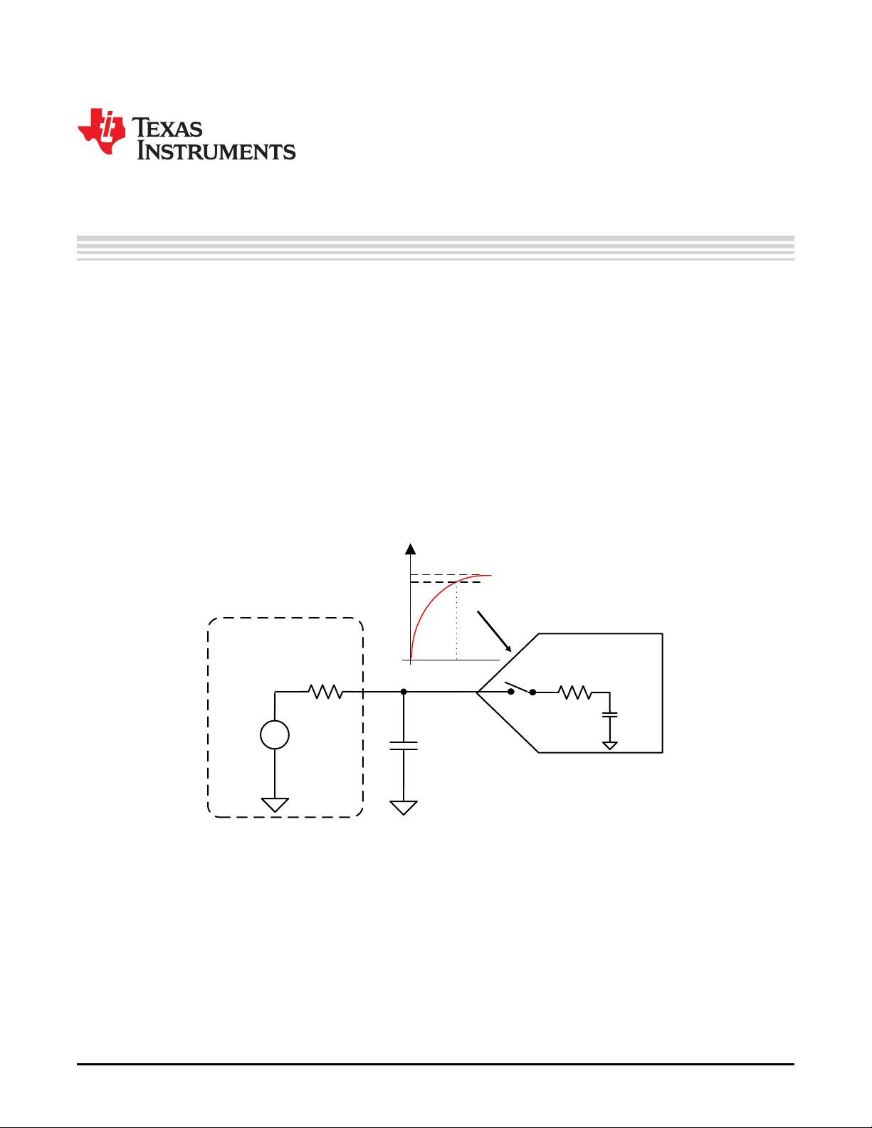
The following figure shows a typical application diagram for interfacing a sensor directly to a SAR ADC
input without the use of a driver amplifier. The sensor block highlights the Thevenin equivalent of a sensor
output. Voltage source, V
TH
, is the Thevenin-equivalent voltage and source resistance R
TH
is the Thevenin-
equivalent impedance. Most sensor data sheets provide the Thevenin model of the sensor from which the
value of the series impedance can be easily calculated.
5
剩余302页未读,继续阅读
春暖花开:)
- 粉丝: 1
- 资源: 4
上传资源 快速赚钱
 我的内容管理
收起
 我的资源
快来上传第一个资源
 我的收益 登录查看自己的收益
 我的积分
登录查看自己的积分
 我的C币
登录后查看C币余额
 我的收藏
我的收藏  我的下载
我的下载  下载帮助
下载帮助

会员权益专享
最新资源
- RTL8188FU-Linux-v5.7.4.2-36687.20200602.tar(20765).gz
- c++校园超市商品信息管理系统课程设计说明书(含源代码) (2).pdf
- 建筑供配电系统相关课件.pptx
- 企业管理规章制度及管理模式.doc
- vb打开摄像头.doc
- 云计算-可信计算中认证协议改进方案.pdf
- [详细完整版]单片机编程4.ppt
- c语言常用算法.pdf
- c++经典程序代码大全.pdf
- 单片机数字时钟资料.doc
- 11项目管理前沿1.0.pptx
- 基于ssm的“魅力”繁峙宣传网站的设计与实现论文.doc
- 智慧交通综合解决方案.pptx
- 建筑防潮设计-PowerPointPresentati.pptx
- SPC统计过程控制程序.pptx
- SPC统计方法基础知识.pptx
资源上传下载、课程学习等过程中有任何疑问或建议,欢迎提出宝贵意见哦~我们会及时处理!
点击此处反馈


安全验证
文档复制为VIP权益,开通VIP直接复制
 信息提交成功
评论0