没有合适的资源?快使用搜索试试~ 我知道了~
首页tps54560数据手册
资源详情
资源评论
资源推荐
SW
VIN
GND
BOOT
FB
COMP
TPS54560
EN
RT/CLK
V
IN
V
OUT
Copyright © 2016, Texas Instruments Incorporated
60
65
70
75
80
85
90
95
100
0 0.5 1 1.5 2 2.5 3 3.5 4 4.5 5
Efficiency (%)
I
O
- Output Current (A)
C024
12 V to 5 V
12 V to 3.3 V
36 V to 12 V
V = 12 V, sw = 800 kHz
OUT
f
V = 5 V and 3.3 V, sw = 400 kHz
OUT
f
Product
Folder
Order
Now
Technical
Documents
Tools &
Software
Support &
Community
An IMPORTANT NOTICE at the end of this data sheet addresses availability, warranty, changes, use in safety-critical applications,
intellectual property matters and other important disclaimers. PRODUCTION DATA.
English Data Sheet: SLVSBN0
TPS54560
ZHCSC58C –MARCH 2013–REVISED MARCH 2017
具具有有 Eco-Mode™ 的的 TPS54560 4.5V 至至 60V 输输入入,,5A 降降压压直直流流/直直流流转转
换换器器
1
1 特特性性
1
• 轻负载条件下使用脉冲跳跃实现的高效率 Eco-
mode。™
• 92mΩ 高侧金属氧化物半导体场效应晶体管
(MOSFET)
• 146μA 静态运行电流和
2μA 关断电流
• 100kHz 至 2.5MHz 的固定开关频率
• 同步至外部时钟
• 轻负载条件下使用集成型引导 (BOOT) 再充电场效
应晶体管 (FET) 实现的低压降
• 可调欠压闭锁 (UVLO) 电压和滞后
• 0.8V 1% 内部电压基准
• 8 引脚 HSOP,带有 PowerPAD™封装
• -40°C 至 150°C T
J
运行范围
•
TPS54560借助 WEBENCH® 电源设计器并使用 创
建定制设计方案
2 应应用用
• 工业自动化和电机控制
• 车辆配件:全球卫星定位系统 (GPS),娱乐系统
• USB 专用充电端口和电池充电器
• 12V,24V 和 48V 工业、汽车和通信电源系统
3 说说明明
TPS54560 是一款配有集成型高侧 MOSFET 的 60V、
5A 降压稳压器。按照 ISO 7637 标准,此器件能够耐
受的抛负载脉冲高达 65V。电流模式控制提供了简单
的外部补偿和灵活的组件选择。一个低纹波脉冲跳跃模
式将无负载时的电源电流减小至 146μA。当启用引脚
被拉至低电平时,关断电源电流被减少至 2μA。
欠压闭锁在内部设定为 4.3V,但可用使能引脚将之提
高。输出电压启动斜升由内部控制以提供一个受控的启
动并且消除过冲。
宽开关频率范围可实现对效率或者外部组件尺寸的优
化。输出电流是受限的逐周期电流。频率折返和热关断
在过载条件下保护内部和外部组件。
TPS54560 可提供 8 引脚热增强型 HSOP
PowerPAD™ 封装。
器器件件信信息息
(1)
订订货货编编号号 封封装装 封封装装尺尺寸寸
TPS54560 HSOP (8) 4.89mm x 3.9mm
(1) 要了解所有可用封装,请见数据表末尾的可订购产品附录。
空白
简简化化电电路路原原理理图图 效效率率与与负负载载电电流流间间的的关关系系
2
TPS54560
ZHCSC58C –MARCH 2013–REVISED MARCH 2017
www.ti.com.cn
版权 © 2013–2017, Texas Instruments Incorporated
目目录录
1 特特性性.......................................................................... 1
2 应应用用.......................................................................... 1
3 说说明明.......................................................................... 1
4 修修订订历历史史记记录录 ........................................................... 2
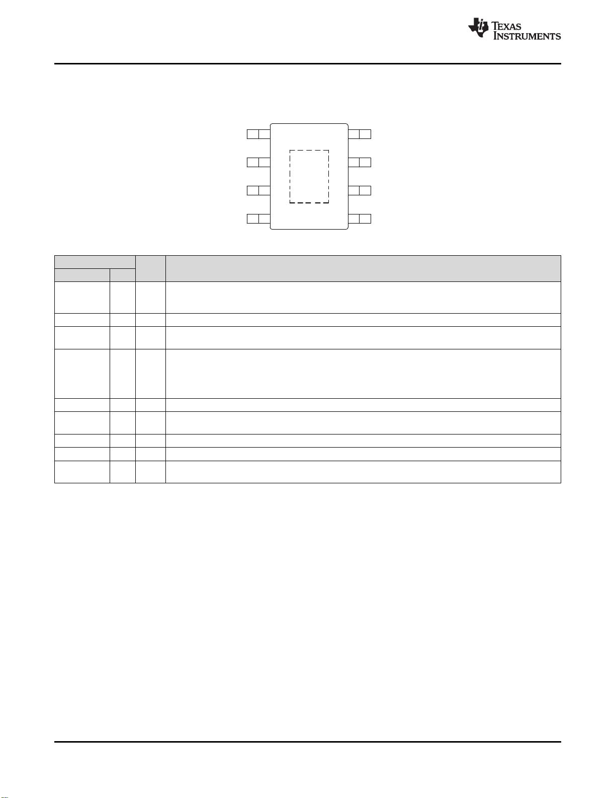
5 Pin Configuration and Functions......................... 4
6 Specifications......................................................... 5
6.1 Absolute Maximum Ratings ...................................... 5
6.2 ESD Ratings.............................................................. 5
6.3 Recommended Operating Conditions....................... 5
6.4 Thermal Information.................................................. 5
6.5 Electrical Characteristics........................................... 6
6.6 Timing Requirements................................................ 7
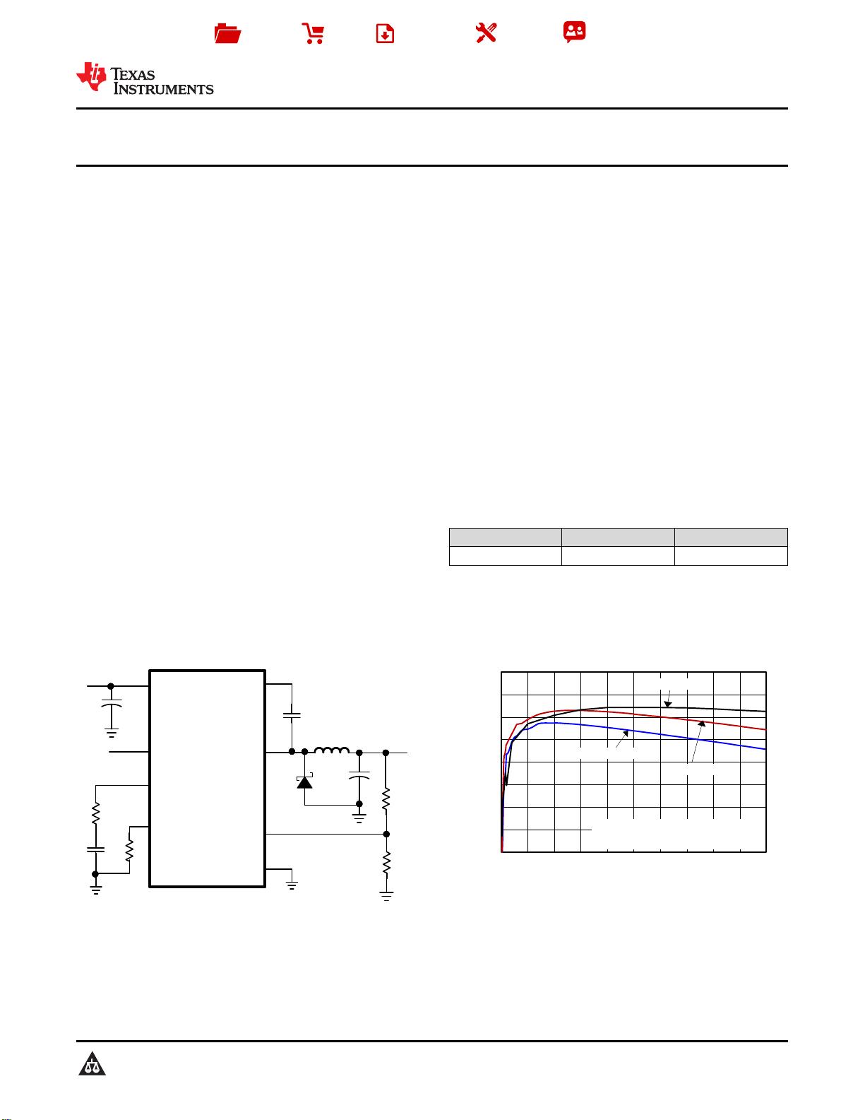
6.7 Typical Characteristics.............................................. 7
7 Detailed Description............................................ 11
7.1 Overview ................................................................. 11
7.2 Functional Block Diagram ....................................... 12
7.3 Feature Description ................................................ 12
7.4 Device Functional Modes........................................ 23
8 Application and Implementation ........................ 24
8.1 Application Information............................................ 24
8.2 Typical Application .................................................. 24
8.3 Inverting Power ....................................................... 37
8.4 Split Rail Power Supply........................................... 37
9 Power Supply Recommendations...................... 38
10 Layout................................................................... 39
10.1 Layout Guidelines ................................................. 39
10.2 Layout Examples................................................... 39
11 器器件件和和文文档档支支持持 ..................................................... 40
11.1 器件支持................................................................ 40
11.2 接收文档更新通知 ................................................. 40
11.3 社区资源................................................................ 40
11.4 商标 ....................................................................... 40
11.5 静电放电警告......................................................... 40
11.6 Glossary................................................................ 40
12 机机械械、、封封装装和和可可订订购购信信息息....................................... 40
4 修修订订历历史史记记录录
Changes from Revision B (August 2016) to Revision C Page
• 更改了 WEBENCH 特性 ......................................................................................................................................................... 1
• Deleted graph: "5V Start/Stop Voltage" from the Typical Characteristics ............................................................................ 10
• Updated text and added Equation 1 in the Low Dropout Operation and Bootstrap Voltage (BOOT) ................................. 13
• Added section: Custom Design with WEBENCH® Tool ..................................................................................................... 25
• Added new section: Minimum Input Voltage, V
IN
................................................................................................................. 30
• Deleted 2 graphs named "Low Dropout Operation" from the Application Curves section ................................................... 33
• 增加了
使用
WEBENCH®
工具定制设计方案
部分................................................................................................................. 40
Changes from Revision A (March 2014) to Revision B Page
• Changed Package type from HSOIC to HSOP ...................................................................................................................... 4
• Moved T
STG
spec from Handling (ESD) ratings table to Absolute Max Ratings table. .......................................................... 5
• Added ± sign to ESD voltages ............................................................................................................................................... 5
• Changed µMhos to µs (Siemens) for the Error Amp specification to align with JEDEC ....................................................... 7
• Changed conditions statement From "V
IN
= 12 V " To "T
A
= 25°C " for Figure 16................................................................. 9
• Changed Equation 7 and Equation 8 ................................................................................................................................... 15
• Added NOTE to Application and Implementation section ................................................................................................... 24
• Changed Equation 27 .......................................................................................................................................................... 25
3
TPS54560
www.ti.com.cn
ZHCSC58C –MARCH 2013–REVISED MARCH 2017
Copyright © 2013–2017, Texas Instruments Incorporated
Changes from Original (March 2013) to Revision A Page
• 已将数据表更改为新的 TI 布局并增加了器件信息表 ............................................................................................................... 1
• Added the Handling Ratings table.......................................................................................................................................... 5
• Added the Recommended Operating Conditions table.......................................................................................................... 5
• Changed the Operating: nonswitching supply current TEST CONDITIONS From: FB = 0.83 V To: FB = 0.9 V .................. 6
• Changed RT/CLK high threshold MAX value From: 1.7 V To: 2 V ....................................................................................... 6
• Changed Figure 6 title From: HIGH FREQUENCY RANGE To: LOW FREQUENCY RANGE ............................................. 7
• Changed Figure 7 title From: LOW FREQUENCY RANGE To: HIGH FREQUENCY RANGE ............................................. 7
• Changed text in the Safe Operating Area ............................................................................................................................ 36
• Added the Power Supply Recommendation section ............................................................................................................ 38
GND7
COMP6
FB5
SW8
2
3
4
1
VIN
EN
RT/CLK
BOOT
PowerPAD
4
TPS54560
ZHCSC58C –MARCH 2013–REVISED MARCH 2017
www.ti.com.cn
Copyright © 2013–2017, Texas Instruments Incorporated
5 Pin Configuration and Functions
HSOP PACKAGE
(TOP VIEW)
Pin Functions
PIN
I/O DESCRIPTION
NAME NO.
BOOT 1 O
A bootstrap capacitor is required between BOOT and SW. If the voltage on this capacitor is below the
minimum required to operate the high side MOSFET, the output is switched off until the capacitor is
refreshed.
VIN 2 I Input supply voltage with 4.5 V to 60 V operating range.
EN 3 I
Enable terminal, with internal pull-up current source. Pull below 1.2 V to disable. Float to enable. Adjust the
input undervoltage lockout with two resistors. See the Enable and Adjusting Undervoltage Lockout section.
RT/CLK 4 I
Resistor Timing and External Clock. An internal amplifier holds this terminal at a fixed voltage when using an
external resistor to ground to set the switching frequency. If the terminal is pulled above the PLL upper
threshold, a mode change occurs and the terminal becomes a synchronization input. The internal amplifier is
disabled and the terminal is a high impedance clock input to the internal PLL. If clocking edges stop, the
internal amplifier is re-enabled and the operating mode returns to resistor frequency programming.
FB 5 I Inverting input of the transconductance (gm) error amplifier.
COMP 6 O
Error amplifier output and input to the output switch current (PWM) comparator. Connect frequency
compensation components to this terminal.
GND 7 – Ground
SW 8 I The source of the internal high-side power MOSFET and switching node of the converter.
Thermal Pad –
GND terminal must be electrically connected to the exposed pad on the printed circuit board for proper
operation.
5
TPS54560
www.ti.com.cn
ZHCSC58C –MARCH 2013–REVISED MARCH 2017
Copyright © 2013–2017, Texas Instruments Incorporated
(1) Stresses beyond those listed under absolute maximum ratings may cause permanent damage to the device. These are stress ratings
only and functional operation of the device at these or any other conditions beyond those indicated under recommended operating
conditions is not implied. Exposure to absolute-maximum-rated conditions for extended periods may affect device reliability.
6 Specifications
6.1 Absolute Maximum Ratings
(1)
over operating free-air temperature range (unless otherwise noted)
MIN MAX UNIT
Input voltage
VIN –0.3 65
V
EN –0.3 8.4
BOOT 73
FB –0.3 3
COMP –0.3 3
RT/CLK –0.3 3.6
Output voltage
BOOT-SW 8
VSW –0.6 65
SW, 10-ns Transient –2 65
Operating junction temperature –40 150 °C
Storage temperature range T
STG
–65 150 °C
(1) Electrostatic discharge (ESD) to measure device sensitivity and immunity to damage caused by assembly line electrostatic discharges
into the device.
(2) Level listed above is the passing level per ANSI/ESDA/JEDEC JS-001. JEDEC document JEP155 states that 500V HBM allows safe
manufacturing with a standard ESD control process. terminals listed as 1000V may actually have higher performance.
(3) Level listed above is the passing level per EIA-JEDEC JESD22-C101. JEDEC document JEP157 states that 250V CDM allows safe
manufacturing with a standard ESD control process. terminals listed as 250V may actually have higher performance.
6.2 ESD Ratings
MIN MAX UNIT
V
ESD
(1)
Human Body Model (HBM) ESD Stress Voltage
(2)
±2000 V
Charged Device Model (HBM) ESD Stress Voltage
(3)
±500 V
(1) See Equation 1
6.3 Recommended Operating Conditions
over operating free-air temperature range (unless otherwise noted)
MIN MAX UNIT
V
IN
Supply input voltage
(1)
V
O
+ V
DO
60 V
V
O
Output voltage 0.8 58.8 V
I
O
Output current 0 5 A
T
J
Junction Temperature –40 150 °C
(1) For more information about traditional and new thermal metrics, see the Semiconductor and IC Package Thermal Metrics application
report.
(2) Power rating at a specific ambient temperature TA should be determined with a junction temperature of 150°C. This is the point where
distortion starts to substantially increase. See power dissipation estimate in application section of this data sheet for more information.
6.4 Thermal Information
THERMAL METRIC
(1)(2)
TPS54560
UNIT
DDA (8 PINS)
θ
JA
Junction-to-ambient thermal resistance (standard board) 42.0 °C/W
ψ
JT
Junction-to-top characterization parameter 5.9 °C/W
ψ
JB
Junction-to-board characterization parameter 23.4 °C/W
θ
JCtop
Junction-to-case(top) thermal resistance 45.8 °C/W
θ
JCbot
Junction-to-case(bottom) thermal resistance 3.6 °C/W
θ
JB
Junction-to-board thermal resistance 23.4 °C/W
剩余47页未读,继续阅读
nyquist0
- 粉丝: 1
- 资源: 3
上传资源 快速赚钱
- 我的内容管理 收起
- 我的资源 快来上传第一个资源
- 我的收益 登录查看自己的收益
- 我的积分 登录查看自己的积分
- 我的C币 登录后查看C币余额
- 我的收藏
- 我的下载
- 下载帮助
会员权益专享
最新资源
- RTL8188FU-Linux-v5.7.4.2-36687.20200602.tar(20765).gz
- c++校园超市商品信息管理系统课程设计说明书(含源代码) (2).pdf
- 建筑供配电系统相关课件.pptx
- 企业管理规章制度及管理模式.doc
- vb打开摄像头.doc
- 云计算-可信计算中认证协议改进方案.pdf
- [详细完整版]单片机编程4.ppt
- c语言常用算法.pdf
- c++经典程序代码大全.pdf
- 单片机数字时钟资料.doc
- 11项目管理前沿1.0.pptx
- 基于ssm的“魅力”繁峙宣传网站的设计与实现论文.doc
- 智慧交通综合解决方案.pptx
- 建筑防潮设计-PowerPointPresentati.pptx
- SPC统计过程控制程序.pptx
- SPC统计方法基础知识.pptx
资源上传下载、课程学习等过程中有任何疑问或建议,欢迎提出宝贵意见哦~我们会及时处理!
点击此处反馈
安全验证
文档复制为VIP权益,开通VIP直接复制
信息提交成功
评论0