没有合适的资源?快使用搜索试试~ 我知道了~
首页VC707_DDR3_datasheet
资源详情
资源评论
资源推荐
DDR3 SDRAM SODIMM
MT8JTF12864HZ – 1GB
MT8JTF25664HZ – 2GB
MT8JTF51264HZ – 4GB
Features
• DDR3 functionality and operations supported as
defined in the component data sheet
• 204-pin, small-outline dual in-line memory module
(SODIMM)
• Fast data transfer rates: PC3-12800, PC3-10600,
PC3-8500, or PC3-6400
• 1GB (128 Meg x 64), 2GB (256 Meg x 64),
4GB (512 Meg x 64)
• V
DD
= 1.5V ±0.075V
• V
DDSPD
= 3.0–3.6V
• Nominal and dynamic on-die termination (ODT) for
data, strobe, and mask signals
• Single-rank
• Serial presence-detect (SPD) EEPROM
• 8 internal device banks
• Fixed burst chop (BC) of 4 and burst length (BL) of 8
via the mode register set (MRS)
• Selectable BC4 or BL8 on-the-fly (OTF)
• Gold edge contacts
• Halogen-free
• Fly-by topology
• Terminated control, command, and address bus
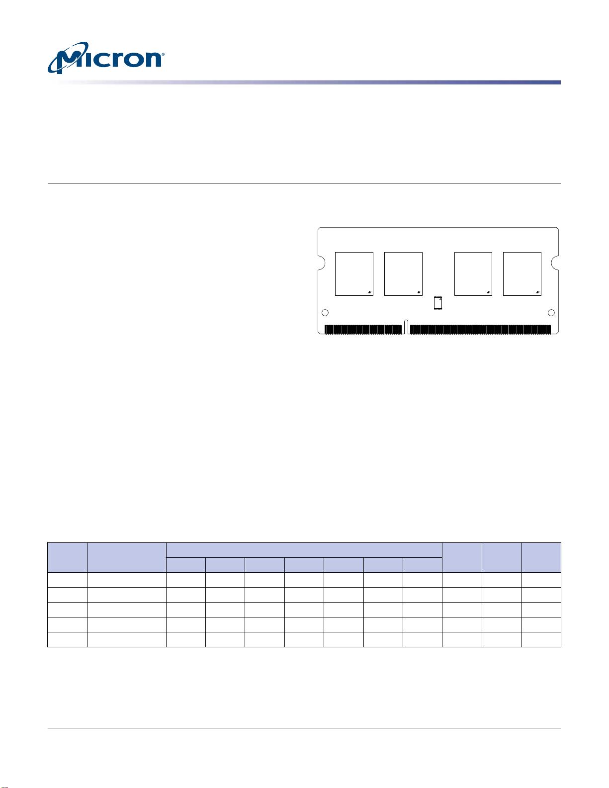
Figure 1: 204-Pin SODIMM (MO-268 R/C B)
Module height: 30mm (1.181in)
Options Marking
• Operating temperature
– Commercial (0°C ≤ T
A
≤ +70°C) None
• Package
– 204-pin DIMM (halogen-free) Z
• Frequency/CAS latency
– 1.25ns @ CL = 11 (DDR3-1600) -1G6
– 1.5ns @ CL = 9 (DDR3-1333) -1G4
– 1.87ns @ CL = 7 (DDR3-1066) -1G1
Table 1: Key Timing Parameters
Speed
Grade
Industry
Nomenclature
Data Rate (MT/s) t
RCD
(ns)
t
RP
(ns)
t
RC
(ns)CL = 11 CL = 10 CL = 9 CL = 8 CL = 7 CL = 6 CL = 5
-1G6 PC3-12800 1600 1333 1333 1066 1066 800 667 13.125 13.125 48.125
-1G4 PC3-10600 – 1333 1333 1066 1066 800 667 13.125 13.125 49.125
-1G1 PC3-8500 – – – 1066 1066 800 667 13.125 13.125 50.625
-1G0 PC3-8500 – – – 1066 – 800 667 15 15 52.5
-80B PC3-6400 – – – – – 800 667 15 15 52.5
1GB, 2GB, 4GB (x64, SR) 204-Pin DDR3 SODIMM
Features
PDF: 09005aef8441a29e
jtf8c128_256_512x64hz.pdf - Rev. G 5/13 EN
1
Micron Technology, Inc. reserves the right to change products or specifications without notice.
© 2010 Micron Technology, Inc. All rights reserved.
Products and specifications discussed herein are subject to change by Micron without notice.
Table 2: Addressing
Parameter 1GB 2GB 4GB
Refresh count 8K 8K 8K
Row address 16K A[13:0] 32K A[14:0] 64K A[15:0]
Device bank address 8 BA[2:0] 8 BA[2:0] 8 BA[2:0]
Device configuration 1Gb (128 Meg x 8) 2Gb (256 Meg x 8) 4Gb (512 Meg x 8)
Column address 1K A[9:0] 1K A[9:0] 1K A[9:0]
Module rank address 1 S0# 1 S0# 1 S0#
Table 3: Part Numbers and Timing Parameters – 1GB Modules
Base device: MT41J128M8,
1
1Gb DDR3 SDRAM
Part Number
2
Module
Density Configuration
Module
Bandwidth
Memory Clock/
Data Rate
Clock Cycles
(CL-
t
RCD-
t
RP)
MT8JTF12864HZ-1G6__ 1GB 128 Meg x 64 12.8 GB/s 1.25ns/1600 MT/s 11-11-11
MT8JTF12864HZ-1G4__ 1GB 128 Meg x 64 10.6 GB/s 1.5ns/1333 MT/s 9-9-9
MT8JTF12864HZ-1G1__ 1GB 128 Meg x 64 8.5 GB/s 1.87ns/1066 MT/s 7-7-7
Table 4: Part Numbers and Timing Parameters – 2GB Modules
Base device: MT41J256M8,
1
2Gb DDR3 SDRAM
Part Number
2
Module
Density Configuration
Module
Bandwidth
Memory Clock/
Data Rate
Clock Cycles
(CL-
t
RCD-
t
RP)
MT8JTF25664HZ-1G6__ 2GB 256 Meg x 64 12.8 GB/s 1.25ns/1600 MT/s 11-11-11
MT8JTF25664HZ-1G4__ 2GB 256 Meg x 64 10.6 GB/s 1.5ns/1333 MT/s 9-9-9
MT8JTF25664HZ-1G1__ 2GB 256 Meg x 64 8.5 GB/s 1.87ns/1066 MT/s 7-7-7
Table 5: Part Numbers and Timing Parameters – 4GB Modules
Base device: MT41J512M8,
1
4Gb DDR3 SDRAM
Part Number
2
Module
Density Configuration
Module
Bandwidth
Memory Clock/
Data Rate
Clock Cycles
(CL-
t
RCD-
t
RP)
MT8JTF51264HZ-1G6__ 4GB 512 Meg x 64 12.8 GB/s 1.25ns/1600 MT/s 11-11-11
MT8JTF51264HZ-1G4__ 4GB 512 Meg x 64 10.6 GB/s 1.5ns/1333 MT/s 9-9-9
MT8JTF51264HZ-1G1__ 4GB 512 Meg x 64 8.5 GB/s 1.87ns/1066 MT/s 7-7-7
Notes:
1. The data sheet for the base device can be found on Micron’s Web site.
2. All part numbers end with a two-place code (not shown) that designates component and PCB revisions.
Consult factory for current revision codes. Example: MT8JTF51264HZ-1G6E1.
1GB, 2GB, 4GB (x64, SR) 204-Pin DDR3 SODIMM
Features
PDF: 09005aef8441a29e
jtf8c128_256_512x64hz.pdf - Rev. G 5/13 EN
2
Micron Technology, Inc. reserves the right to change products or specifications without notice.
© 2010 Micron Technology, Inc. All rights reserved.
Pin Assignments
Table 6: Pin Assignments
204-Pin DDR3 SODIMM Front 204-Pin DDR3 SODIMM Back
Pin Symbol Pin Symbol Pin Symbol Pin Symbol Pin Symbol Pin Symbol Pin Symbol Pin Symbol
1 V
REFDQ
53 DQ19 105 V
DD
157 DQ42 2 V
SS
54 V
SS
106 V
DD
158 DQ46
3 V
SS
55 V
SS
107 A10 159 DQ43 4 DQ4 56 DQ28 108 BA1 160 DQ47
5 DQ0 57 DQ24 109 BA0 161 V
SS
6 DQ5 58 DQ29 110 RAS# 162 V
SS
7 DQ1 59 DQ25 111 V
DD
163 DQ48 8 V
SS
60 V
SS
112 V
DD
164 DQ52
9 V
SS
61 V
SS
113 WE# 165 DQ49 10 DQS0# 62 DQ3# 114 S0# 166 DQ53
11 DM0 63 DM3 115 CAS# 167 V
SS
12 DQS0 64 DQ3 116 ODT0 168 V
SS
13 V
SS
65 V
SS
117 V
DD
169 DQS6# 14 V
SS
66 V
SS
118 V
DD
170 DM6
15 DQ2 67 DQ26 119 A13 171 DQS6 16 DQ6 68 DQ30 120 NC 172 V
SS
17 DQ3 69 DQ27 121 NC 173 V
SS
18 DQ7 70 DQ31 122 NC 174 DQ54
19 V
SS
71 V
SS
123 V
DD
175 DQ50 20 V
SS
72 V
SS
124 V
DD
176 DQ55
21 DQ8 73 CKE0 125 NC 177 DQ51 22 DQ12 74 NC 126 V
REFCA
178 V
SS
23 DQ9 75 V
DD
127 V
SS
179 V
SS
24 DQ13 76 V
DD
128 V
SS
180 DQ60
25 V
SS
77 NC 129 DQ32 181 DQ56 26 V
SS
78 A15 130 DQ36 182 DQ61
27 DQS1# 79 BA2 131 DQ33 183 DQ57 28 DM1 80 A14 132 DQ37 184 V
SS
29 DQS1 81 V
DD
133 V
SS
185 V
SS
30 RESET# 82 V
DD
134 V
SS
186 DQS7#
31 V
SS
83 A12 135 DQS4# 187 DM7 32 V
SS
84 A11 136 DM4 188 DQS7
33 DQ10 85 A9 137 DQS4 189 V
SS
34 DQ14 86 A7 138 V
SS
190 V
SS
35 DQ11 87 V
DD
139 V
SS
191 DQ58 36 DQ15 88 V
DD
140 DQ38 192 DQ62
37 V
SS
89 A8 141 DQ34 193 DQ59 38 V
SS
90 A6 142 DQ39 194 DQ63
39 DQ16 91 A5 143 DQ35 195 V
SS
40 DQ20 92 A4 144 V
SS
196 V
SS
41 DQ17 93 V
DD
145 V
SS
197 SA0 42 DQ21 94 V
DD
146 DQ44 198 NF
43 V
SS
95 A3 147 DQ40 199 V
DDSPD
44 V
SS
96 A2 148 DQ45 200 SDA
45 DQS2# 97 A1 149 DQ41 201 SA1 46 DM2 98 A0 150 V
SS
202 SCL
47 DQS2 99 V
DD
151 V
SS
203 V
TT
48 V
SS
100 V
DD
152 DQS5# 204 V
TT
49 V
SS
101 CK0 153 DM5 – – 50 DQ22 102 CK1 154 DQS5 – –
51 DQ18 103 CK0# 155 V
SS
– – 52 DQ23 104 CK1# 156 V
SS
– –
1GB, 2GB, 4GB (x64, SR) 204-Pin DDR3 SODIMM
Pin Assignments
PDF: 09005aef8441a29e
jtf8c128_256_512x64hz.pdf - Rev. G 5/13 EN
3
Micron Technology, Inc. reserves the right to change products or specifications without notice.
© 2010 Micron Technology, Inc. All rights reserved.
Pin Descriptions
The pin description table below is a comprehensive list of all possible pins for all DDR3
modules. All pins listed may not be supported on this module. See Pin Assignments for
information specific to this module.
Table 7: Pin Descriptions
Symbol Type Description
Ax Input Address inputs: Provide the row address for ACTIVE commands, and the column ad-
dress and auto precharge bit (A10) for READ/WRITE commands, to select one location
out of the memory array in the respective bank. A10 sampled during a PRECHARGE
command determines whether the PRECHARGE applies to one bank (A10 LOW, bank
selected by BAx) or all banks (A10 HIGH). The address inputs also provide the op-code
during a LOAD MODE command. See the Pin Assignments Table for density-specific
addressing information.
BAx Input Bank address inputs: Define the device bank to which an ACTIVE, READ, WRITE, or
PRECHARGE command is being applied. BA define which mode register (MR0, MR1,
MR2, or MR3) is loaded during the LOAD MODE command.
CKx,
CKx#
Input Clock: Differential clock inputs. All control, command, and address input signals are
sampled on the crossing of the positive edge of CK and the negative edge of CK#.
CKEx Input Clock enable: Enables (registered HIGH) and disables (registered LOW) internal circui-
try and clocks on the DRAM.
DMx Input Data mask (x8 devices only): DM is an input mask signal for write data. Input data
is masked when DM is sampled HIGH, along with that input data, during a write ac-
cess. Although DM pins are input-only, DM loading is designed to match that of the
DQ and DQS pins.
ODTx Input On-die termination: Enables (registered HIGH) and disables (registered LOW) termi-
nation resistance internal to the DDR3 SDRAM. When enabled in normal operation,
ODT is only applied to the following pins: DQ, DQS, DQS#, DM, and CB. The ODT input
will be ignored if disabled via the LOAD MODE command.
Par_In Input Parity input: Parity bit for Ax, RAS#, CAS#, and WE#.
RAS#, CAS#, WE# Input Command inputs: RAS#, CAS#, and WE# (along with S#) define the command being
entered.
RESET# Input
(LVCMOS)
Reset: RESET# is an active LOW asychronous input that is connected to each DRAM
and the registering clock driver. After RESET# goes HIGH, the DRAM must be reinitial-
ized as though a normal power-up was executed.
Sx# Input Chip select: Enables (registered LOW) and disables (registered HIGH) the command
decoder.
SAx Input Serial address inputs: Used to configure the temperature sensor/SPD EEPROM ad-
dress range on the I
2
C bus.
SCL Input Serial clock for temperature sensor/SPD EEPROM: Used to synchronize communi-
cation to and from the temperature sensor/SPD EEPROM on the I
2
C bus.
CBx I/O Check bits: Used for system error detection and correction.
DQx I/O Data input/output: Bidirectional data bus.
DQSx,
DQSx#
I/O Data strobe: Differential data strobes. Output with read data; edge-aligned with
read data; input with write data; center-aligned with write data.
1GB, 2GB, 4GB (x64, SR) 204-Pin DDR3 SODIMM
Pin Descriptions
PDF: 09005aef8441a29e
jtf8c128_256_512x64hz.pdf - Rev. G 5/13 EN
4
Micron Technology, Inc. reserves the right to change products or specifications without notice.
© 2010 Micron Technology, Inc. All rights reserved.
剩余15页未读,继续阅读
小坏坏大坏蛋
- 粉丝: 0
- 资源: 2
上传资源 快速赚钱
- 我的内容管理 收起
- 我的资源 快来上传第一个资源
- 我的收益 登录查看自己的收益
- 我的积分 登录查看自己的积分
- 我的C币 登录后查看C币余额
- 我的收藏
- 我的下载
- 下载帮助
会员权益专享
最新资源
- zigbee-cluster-library-specification
- JSBSim Reference Manual
- c++校园超市商品信息管理系统课程设计说明书(含源代码) (2).pdf
- 建筑供配电系统相关课件.pptx
- 企业管理规章制度及管理模式.doc
- vb打开摄像头.doc
- 云计算-可信计算中认证协议改进方案.pdf
- [详细完整版]单片机编程4.ppt
- c语言常用算法.pdf
- c++经典程序代码大全.pdf
- 单片机数字时钟资料.doc
- 11项目管理前沿1.0.pptx
- 基于ssm的“魅力”繁峙宣传网站的设计与实现论文.doc
- 智慧交通综合解决方案.pptx
- 建筑防潮设计-PowerPointPresentati.pptx
- SPC统计过程控制程序.pptx
资源上传下载、课程学习等过程中有任何疑问或建议,欢迎提出宝贵意见哦~我们会及时处理!
点击此处反馈
安全验证
文档复制为VIP权益,开通VIP直接复制
信息提交成功
评论0