没有合适的资源?快使用搜索试试~ 我知道了~
首页sx1301 lora网关芯片
资源详情
资源评论
资源推荐

SX1301
WIRELESS & SENSING PRODUCTS Datasheet
V2.3 May 2017 www.semtech.com 1
DDR -
LoRa
DDR
-
LoRa
DDR -
LoRa
8x
LoRa
(G)FSK
(G)FSK/LoRa
Packet handler
MCU
SX1301
SPI
Packet
handler
Control
Tx/Rx
(Tx/Rx)
(GPS)
I/Q
I/Q
I/Q
I/Q
timestamp
General Description
The SX1301 digital baseband chip is a massive
digital signal processing engine specifically
designed to offer breakthrough gateway
capabilities in the ISM bands worldwide. It
integrates the LoRa concentrator IP.
The LoRa concentrator is a multi-channel high
performance transmitter/receiver designed to
simultaneously receive several LoRa packets
using random spreading factors on random
channels. Its goal is to enable robust
connection between a central wireless data
concentrator and a massive amount of
wireless end-points spread over a very wide
range of distances.
The SX1301 is targeted at smart metering
fixed networks and Internet of Things
applications.
Ordering Information
Part Number
Conditioning
SX1301IMLTRC
Tape & Reel
3,000 parts per reel
SX1301IMLTRT
Tape & Reel
500 parts per reel
Key product features
• Up to -142 dBm sensitivity with SX1257
or SX1255 Tx/Rx front-end
• -139.5 dBm with included ref
design
• 70 dB CW interferer rejection at
1 MHz offset
• Able to operate with negative SNR
• CCR up to 9 dB
• Emulates 49x LoRa demodulators and 1x
(G)FSK demodulator
• Dual digital Tx & Rx radio front-end
interfaces
• 10 programmable parallel demodulation
paths
• Dynamic data-rate adaptation (ADR)
• True antenna diversity or simultaneous
dual-band operation
Applications
• Smart Metering
• Security Sensors Network
• Agricultural Monitoring
• Internet of Things (IoT)

SX1301
WIRELESS & SENSING PRODUCTS Datasheet
V2.3 May 2017 www.semtech.com 2
Contents
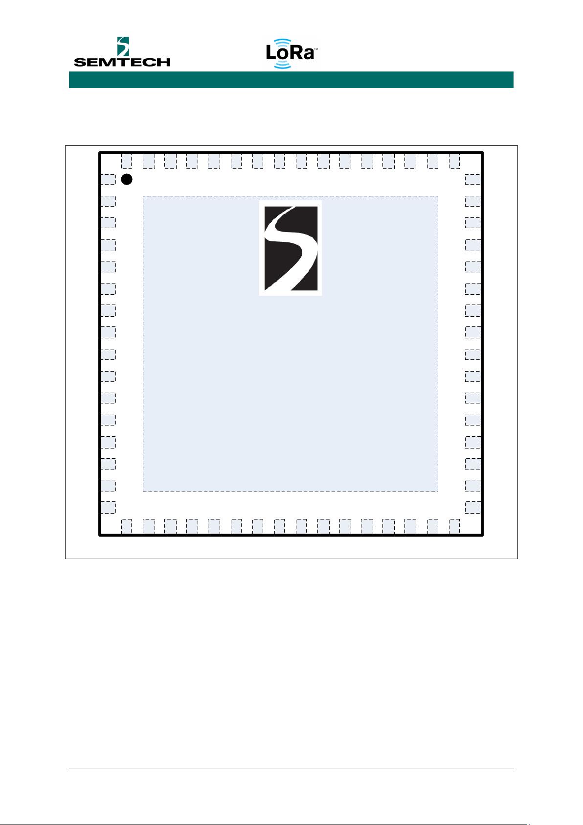
1 PIN CONFIGURATION .................................................................................................................. 4
1.1 Pins placement and circuit marking ............................................................................................ 4
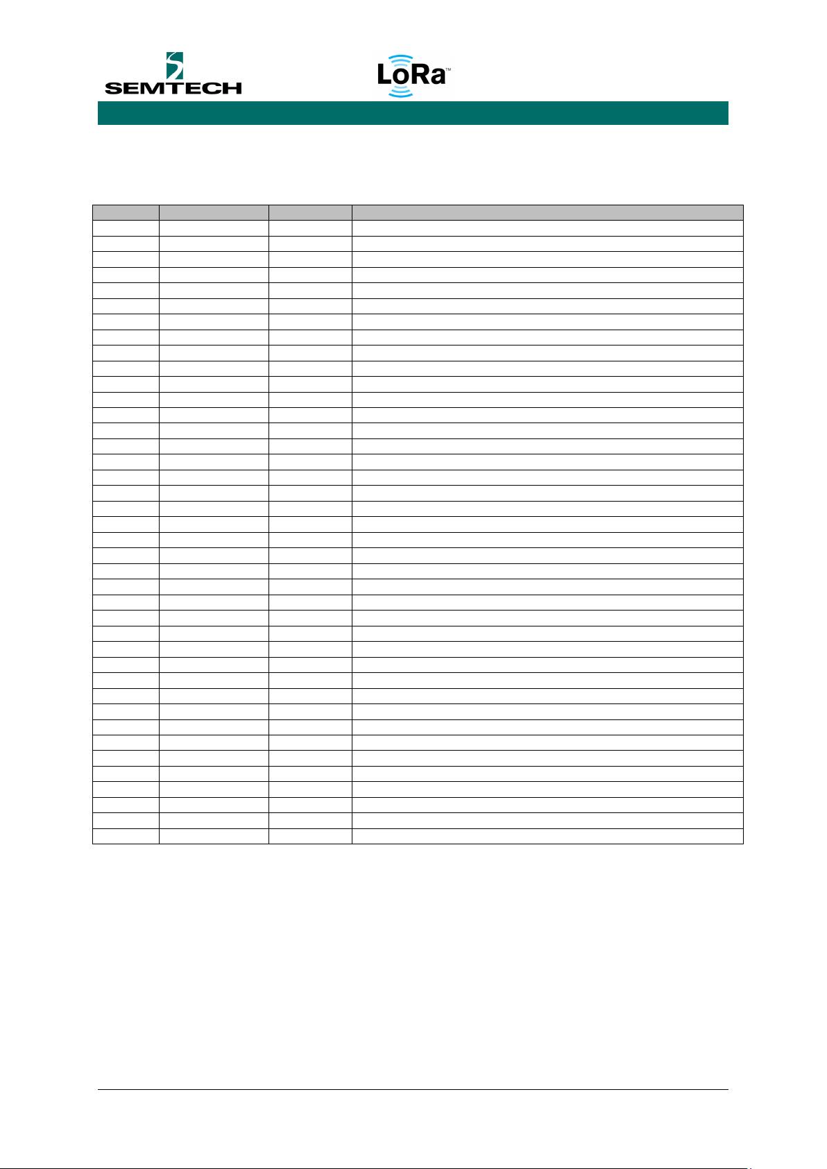
1.2 Pins description ........................................................................................................................... 5
2 ELECTRICAL CHARACTERISTICS ................................................................................................... 7
2.1 Absolute maximum ratings ......................................................................................................... 7
2.2 Constraints on external ............................................................................................................... 7
2.3 Operating conditions .................................................................................................................. 7
2.4 Electrical specifications ............................................................................................................... 8
2.5 Timing specifications ................................................................................................................... 8
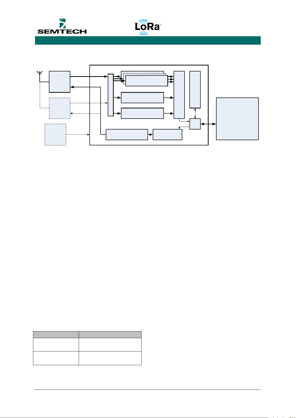
3 CIRCUIT OPERATION ................................................................................................................... 9
3.1 General Presentation .................................................................................................................. 9
3.2 Power-on ..................................................................................................................................... 9
3.2.1 Power-up sequence ................................................................................................................ 9
3.2.2 Setting the circuit is low-power mode .................................................................................... 9
3.3 Clocking ..................................................................................................................................... 10
3.4 SPI Interface .............................................................................................................................. 11
3.5 Rx I/Q Interface ......................................................................................................................... 12
3.5.1 I/Q generated on clock rising edge ....................................................................................... 12
3.5.2 I/Q generated on clock falling edge ...................................................................................... 12
3.6 RX mode block diagram, reception paths characteristics ......................................................... 13
3.6.1 Block diagram ........................................................................................................................ 13
3.6.2 Reception paths characteristics ............................................................................................ 13
3.7 Packet engine and data buffers ................................................................................................ 15
3.7.1 Receiver Packet engine ......................................................................................................... 15
3.7.2 Transmitter packet engine .................................................................................................... 17
3.8 Receiver IF frequencies configuration ...................................................................................... 19
3.8.1 Configuration using 2 x SX1257 radios .................................................................................. 19
3.8.2 Two SX1255 : 433 MHz band ................................................................................................ 21
3.8.3 One SX1257 and one SX1255 ................................................................................................ 21
3.9 Connection to RF front-end ...................................................................................................... 22
3.9.1 Connection to Semtech SX1255 or SX1257 components ..................................................... 22
3.9.2 SX1301 RX operation using a third party RF front-end ......................................................... 22
3.9.3 Radio calibration ................................................................................................................... 24
3.9.4 SX1301 connection to RF front-end for TX operation ........................................................... 24
3.10 Reference application ............................................................................................................... 26
3.11 SX1301 sensitivity performance in reference application ........................................................ 27
3.12 SX1301 sensitivity vs data rate in LoRa mode........................................................................... 28
3.12.1 125kHz mode: IF8, IF[0 to 7] paths ....................................................................................... 28
3.12.2 250 & 500 kHz mode: IF8 only .............................................................................................. 29
3.13 SX1301 interference rejection .................................................................................................. 29
3.14 Hardware Abstraction Layer (HAL) ........................................................................................... 31
3.14.1 Introduction .......................................................................................................................... 31
3.14.2 Abstraction presented to the gateway host ......................................................................... 32
4 EXTERNAL COMPONENTS ......................................................................................................... 33
5 PCB LAYOUT CONSIDERATIONS ................................................................................................ 34

SX1301
WIRELESS & SENSING PRODUCTS Datasheet
V2.3 May 2017 www.semtech.com 3
6 PACKAGING INFORMATION ...................................................................................................... 37
6.1 Package Outline Drawing .......................................................................................................... 37
6.2 Thermal impedance of package ................................................................................................ 37
6.3 Land Pattern Drawing ............................................................................................................... 38
7 REVISION INFORMATION .......................................................................................................... 39
Figures
Figure 1 Top view of SX1301 package with 64 pins and exposed ground paddle (bottom of package). 4
Figure 2 Power-up sequence .................................................................................................................. 9
Figure 3 SPI Timing Diagram (single access) ......................................................................................... 11
Figure 4 I/Q on clock rising edge ........................................................................................................... 12
Figure 5 I/Q on clock falling edge .......................................................................................................... 12
Figure 6 SX1301 digital baseband chip block diagram .......................................................................... 13
Figure 7 Access FIFO and data buffer ................................................................................................... 16
Figure 8 SX1255/57 digital I/Q power spectral density ........................................................................ 19
Figure 9 Radio spectrum ....................................................................................................................... 20
Figure 10 Radio spectrum ..................................................................................................................... 20
Figure 11 Radio spectrum ..................................................................................................................... 21
Figure 12 Dual band operation ............................................................................................................. 22
Figure 13 SX1301 with third party frontend ......................................................................................... 23
Figure 14 Digital interface for third party radio .................................................................................... 23
Figure 15 Transmission schematics ...................................................................................................... 24
Figure 16 Reference application ........................................................................................................... 26
Figure 17 CW interferer rejection @ SF7 for 50% PER at sensitivity + 3dB .......................................... 30
Figure 18 CW interferer rejection @ SF12 for 50% PER at sensitivity + 3dB ........................................ 30
Figure 19 EPCOS B3117 SAW filter transfer function ........................................................................... 31
Figure 20 PCB layout example .............................................................................................................. 36
Figure 21 Package dimensions .............................................................................................................. 37
Figure 22 Land pattern drawing ............................................................................................................ 38
Tables
Table 1 Pins name and description ......................................................................................................... 6
Table 2 Absolute maximum ratings ........................................................................................................ 7
Table 3 Externals ..................................................................................................................................... 7
Table 4 Operating conditions for electrical specifications ...................................................................... 7
Table 5 Electrical specifications .............................................................................................................. 8
Table 6 Timing specifications .................................................................................................................. 8
Table 7 Packet data fields ..................................................................................................................... 17
Table 8 Packet structure for transmission ............................................................................................ 18
Table 9 IF frequencies set ..................................................................................................................... 20
Table 10 IF frequency used ................................................................................................................... 21
Table 11 SX1301 performance in reference application ...................................................................... 27
Table 12 Sensitivity with 125 kHz mode ............................................................................................... 28
Table 13 Sensitivity with 250 kHz mode ............................................................................................... 29
Table 14 Sensitivity with 500 kHz mode ............................................................................................... 29
Table 15 Recommended external components .................................................................................... 33

SX1301
WIRELESS & SENSING PRODUCTS Datasheet
V2.3 May 2017 www.semtech.com 4
1 Pin Configuration
1.1 Pins placement and circuit marking
1
16
17
32
64
49
48
33
SX1301
yyww
xxxxxxxx
Legend: yyww is the date code and xxxxxxxx is the Semtech lot number.
Figure 1 Top view of SX1301 package with 64 pins and exposed ground paddle (bottom of package).
The ground paddle must be connected to ground potential through a large conductive plane that
also serves for temperature dissipation.

SX1301
WIRELESS & SENSING PRODUCTS Datasheet
V2.3 May 2017 www.semtech.com 5
1.2 Pins description
The table below gives the description of the pins of the circuit.
Pin
Pin Name
Type
Description
0
VSS
Power (GND)
Ground paddle – must be connected to ground for thermal dissipation
1
RESET
Input
Global asynchronous reset
2
HOST_SCK
Input
HOST SPI clock (max 10 MHz clock)
3
HOST_MISO
Output
HOST SPI Interface
4
HOST_MOSI
Input
HOST SPI Interface
5
HOST_CSN
Input
HOST SPI Interface
6
SCANMODE
Input
Scanmode signal (tied to 0 in normal mode)
7
VSS
Power (GND)
Ground
8
VCC18
Power (VDD)
Logic core supply
9
GPS_IN
Input
GPS 1 pps input
10
VSS
Power (GND)
Ground
11
VSS
Power (GND)
Ground
12
VCC18
Power (VDD)
Logic core supply
13
RADIO_A_EN
Output
Radio A global enable
14
LNA_A_CTRL
Output
LNA A enable
15
PA_A_CTRL
Output
PA A enable
16
NC
No connected – tie to VSS
17
PA_GAIN[1]
Output
PA gain control of both radio A/B
18
PA_GAIN[0]
Output
PA gain control of both radio A/B
19
RADIO_B_CS
Output
Radio B SPI interface
20
RADIO_B_MOSI
Output
Radio B SPI interface
21
RADIO_B_MISO
Input
Radio B SPI interface
22
RADIO_B_SCK
Output
Radio B SPI interface
23
VCC18
Power (VCC)
Logic core supply
24
VSS
Power (GND)
Ground
25
RADIO_RST
Output
Radio A/B global reset
26
PA_B_CTRL
Output
PA B enable
27
LNA_B_CTRL
Output
LNA B enable
28
RADIO_B_EN
Output
Radio B global enable
29
VCC33
Power (VCC)
Logic IO supply
30
VSS
Power (GND)
Ground
31
VSS
Power (GND)
Ground
32
NC
No connected – tie to VSS
33
NC
No connected – tie to VSS
34
SP_VALID
Input
Radio C sample valid
35
B_IQ_RX
Input
Radio B 1 bit I/Q Rx samples
36
B_QI_RX
Input
Radio B 1 bit Q/I Rx samples
37
B_IQ_TX
Output
Radio B 1 bit I/Q Tx samples
38
B_QI_TX
Output
Radio B 1 bit Q/I Tx samples
39
SP_CLK_OUT
Output
Radio C clock out (32 MHz)
剩余39页未读,继续阅读


安全验证
文档复制为VIP权益,开通VIP直接复制

评论0