
© 2004 Device Engineering Inc.
DS-MP-00429 Rev. F
03/11/2004
1 of 12
Device
Engineering
Incorporated
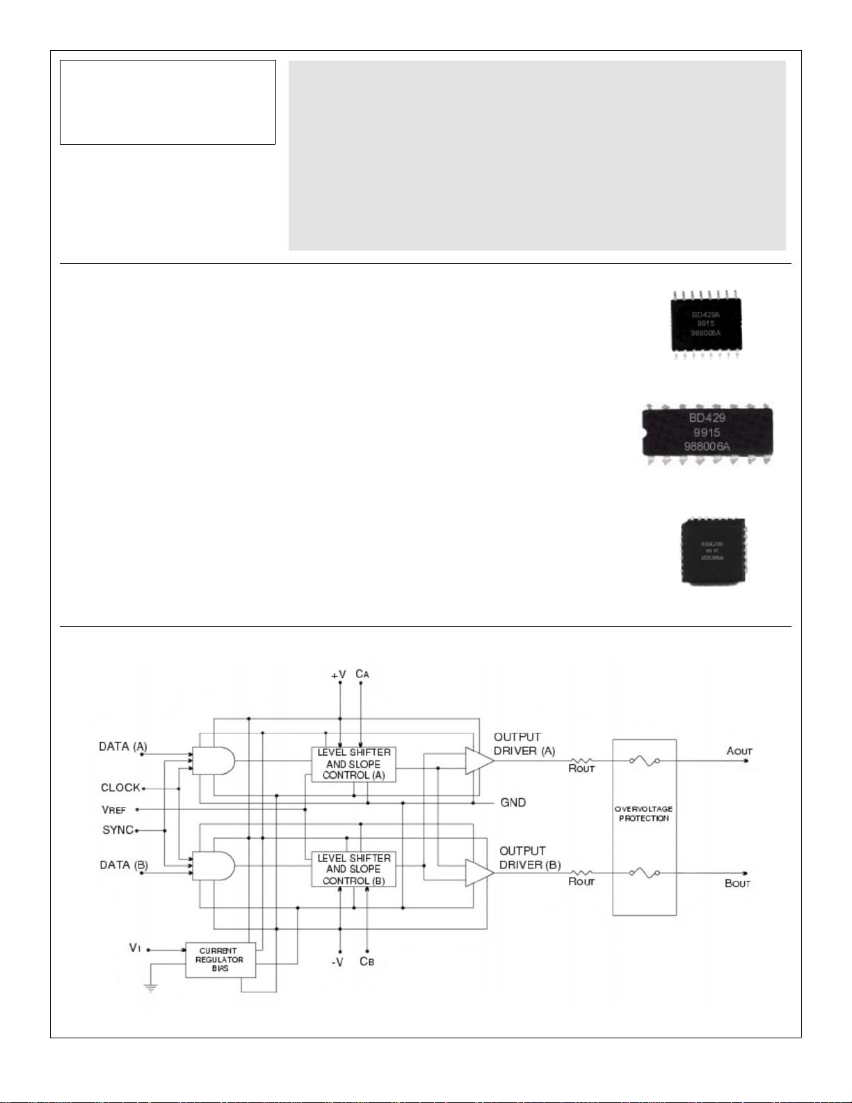
BD429/BD429A/BD429B
ARINC 429/RS-422 Line Driver
Integrated Circuit
385 E. Alamo Drive
Chandler, AZ 85225
Phone: (480) 303-0822
Fax: (480) 303-0824
E-mail: admin@deiaz.com
Features:
• ARINC 429 Line Driver for HI speed (100 kHz) and LOW speed (12.5 kHz) data rates
• Pin for Pin replacement part for industry standard ARINC 429 Line Drivers
• Available in a 16 Pin SOIC (WB), 16 Pin CERDIP, 16 Pin Plastic Dip,
16 Lead Ceramic SOP, and 28L PLCC
• Low EMI RS-422 line driver mode for data rates up to 100 kHz
• Adjustable slew rates via two external capacitors
• Inputs are TTL and CMOS compatible
• Low quiescent power of 125mW (typical)
• Programmable output differential range via V
REF
pin
• Outputs are fused for failsafe overvoltage protection
• Drives full ARINC load of 400Ω and 30,000pF
• Extended (-55°C/+85°C) and Military (-55°C/+125°C) temperature ranges
• 100% Final Testing
Figure 1: BD429 Block Diagram

剩余11页未读,继续阅读

幽郁普林斯
- 粉丝: 4
- 资源: 4
 我的内容管理
收起
我的内容管理
收起
- 我的资源
快来上传第一个资源
 我的收益 登录查看自己的收益
 我的积分
登录查看自己的积分
我的积分
登录查看自己的积分
 我的C币
登录后查看C币余额
我的C币
登录后查看C币余额
 我的收藏
我的收藏  我的下载
我的下载  下载帮助
下载帮助

会员权益专享


最新资源
- zigbee-cluster-library-specification
- JSBSim Reference Manual
- c++校园超市商品信息管理系统课程设计说明书(含源代码) (2).pdf
- 建筑供配电系统相关课件.pptx
- 企业管理规章制度及管理模式.doc
- vb打开摄像头.doc
- 云计算-可信计算中认证协议改进方案.pdf
- [详细完整版]单片机编程4.ppt
- c语言常用算法.pdf
- c++经典程序代码大全.pdf
- 单片机数字时钟资料.doc
- 11项目管理前沿1.0.pptx
- 基于ssm的“魅力”繁峙宣传网站的设计与实现论文.doc
- 智慧交通综合解决方案.pptx
- 建筑防潮设计-PowerPointPresentati.pptx
- SPC统计过程控制程序.pptx
资源上传下载、课程学习等过程中有任何疑问或建议,欢迎提出宝贵意见哦~我们会及时处理!
点击此处反馈


评论0