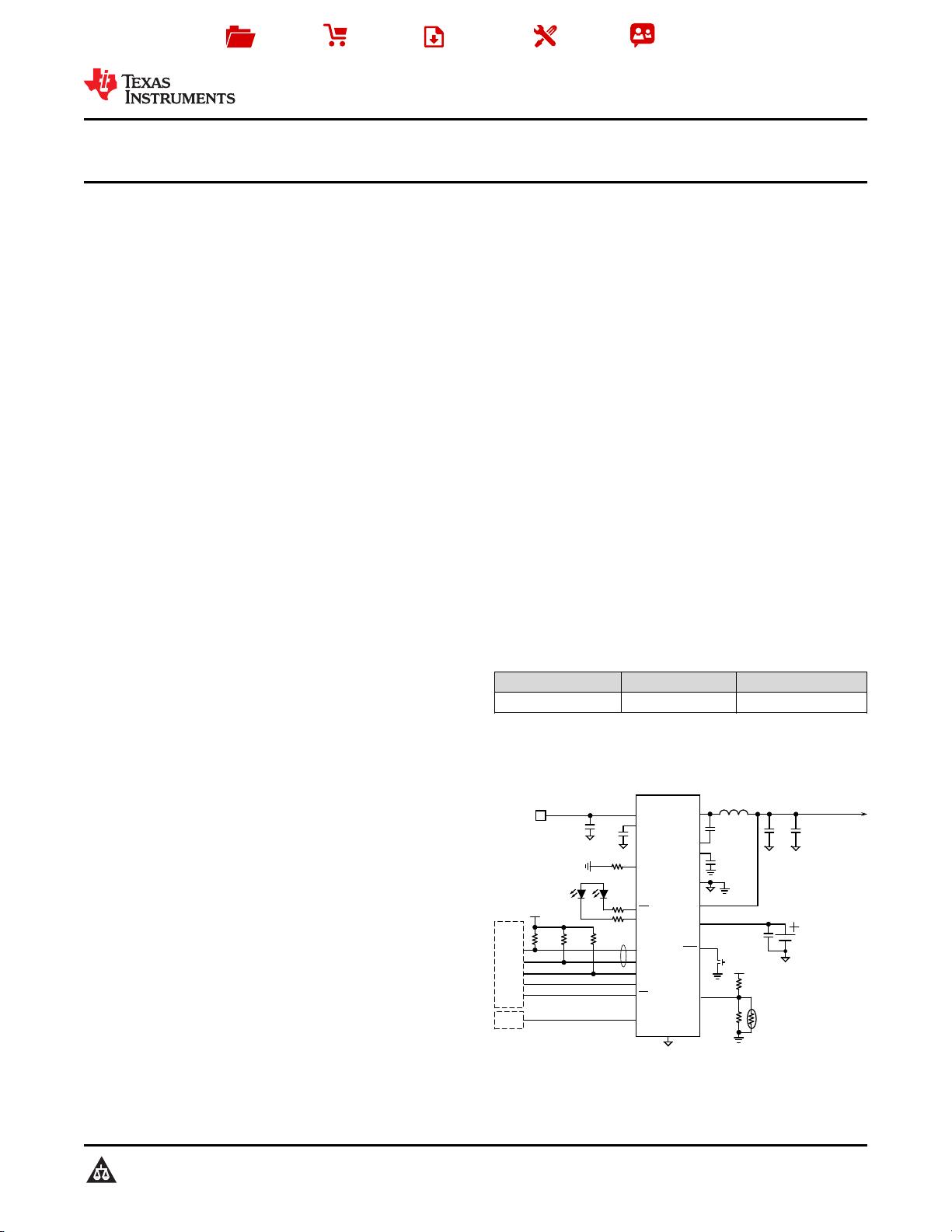
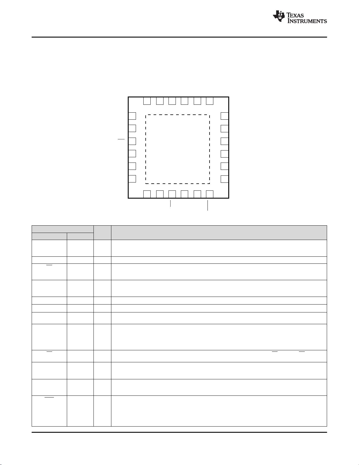
没有合适的资源?快使用搜索试试~ 我知道了~
首页BQ24298USB 充电器 datasheet 电路参考图
BQ24298USB 充电器 datasheet 电路参考图
需积分: 9 16 下载量 191 浏览量
更新于2023-05-31
评论
收藏 1.08MB PDF 举报
bq24298 具有窄范围 VDC 电源路径管理和可调电压 USB OTG 的 I2C 控制 3A 单节 USB 充电器
资源详情
资源评论
资源推荐
VBUS
PMID
SDA
SCL
INT
OTG
CE
PSEL
SW
BOOT
REGN
PGND
SYS
BAT
ILIM
TS
SYS: 3.5V-4.35V
5V USB
SDP/DCP
bq24298
Thermal Pad
REGN
1 Fμ
8.2
μF
47nF
4.7 Fμ
1 Hμ
10μF
317W
(1.5A max)
VREF
10kW
10kW
10kW
STAT
PG
SYS
2.2kW
PHY
Host
10 Fμ
10 Fμ
QON
4.2V
5.25kW
31.23kW
10kW
Charge Enable (0°C - 45°C)
Product
Folder
Sample &
Buy
Technical
Documents
Tools &
Software
Support &
Community
bq24298
ZHCSDK7 –APRIL 2015
bq24298 具具有有窄窄范范围围 VDC 电电源源路路径径管管理理和和可可调调电电压压 USB OTG 的的 I
2
C 控控制制
3A 单单节节 USB 充充电电器器
1
1 特特性性
• 90% 高效开关模式 3A 充电器 – 热调节和热关断
• 3.9V 至 6.2V 单输入 USB 标准充电器,提供 6.4V
– 输入和系统过压保护
过压保护
– MOSFET 过流保护
– 输入电压和电流限制支持 USB 2.0 和 USB 3.0
• 针对 LED 或主机处理器的充电状态输出
– 输入电流限值:
• 通过输入电压稳压实现的最大功率跟踪功能
100mA,150mA,500mA,900mA,1A,
• 20µA 低电池泄漏电流,支持运输模式和系统复位
1.5A,2A 和 3A
• I
2
C 强制 BATFET 关闭延迟(典型值 9s)
• USB OTG 1A 或 1.5A 时可调输出电压范围为
• 4.00mm x 4.00mm 超薄四方扁平无引线 (WQFN)-
4.55V 至 5.5V
24 封装
– 快速 OTG 启动(典型值 22ms)
– 5V 升压模式效率为 90%
2 应应用用
– 精确的 ±15% 断续模式过流保护
• 平板电脑,智能手机,网络设备
• 窄范围 VDC (NVDC) 电源路径管理
• 便携式音频扬声器
– 在无电池或深度电池放电时的即时系统启动
3 说说明明
– 电池充电模式中的理想二极管运行
• 薄型 1.2mm 电感 1.5MHz 开关频率
bq24298 是一款高度集成开关模式电池充电管理和系
• I
2
C 端口用于实现最优系统性能和状态报告
统电源路径管理器件,此器件用于续航各种智能手机和
• 具有或不具有主机管理的自主电池充电
平板电脑应用中的单节锂离子和锂聚合物电池。 它的
低阻抗电源路径对开关模式运行效率进行了优化、减少
– 电池充电使能
了电池充电时间并延长了放电阶段的电池寿命。
– 电池充电预调节
– 充电终止和再充电
器器件件信信息息
(1)
• 高精度
器器件件型型号号 封封装装 封封装装尺尺寸寸((标标称称值值))
– ±0.5% 充电电压调节
bq24298 WQFN (24) 4.00mm x 4.00mm
– 充电电流调节范围为 ±7%
(1) 如需了解所有可用封装,请见数据表末尾的可订购产品附录。
– 输入电流调节范围为 ±7.5%
PSEL 连连接接 PHY,,通通过过 SDP/DCP 充充电电并并带带有有可可选选
– USB OTG 升压模式下 ± 3% 输出电压调节范围
BATFET 使使能能接接口口
• 高集成
– 电源路径管理
– 同步开关 MOSFET
– 集成电流感测
– 阴极负载二极管
– 内部环路补偿
• 安全性
– 针对 OTG 模式中充电和放电的电池温度感测
– 电池充电安全定时器
1
PRODUCTION DATA information is current as of publication date. Products conform to specifications per the terms of the Texas
Instruments standard warranty. Production processing does not necessarily include testing of all parameters.
English Data Sheet: SLUSC59
bq24298
ZHCSDK7 –APRIL 2015
www.ti.com.cn
目目录录
8.4 Device Functional Modes........................................ 25
1 特特性性.......................................................................... 1
8.5 Programming........................................................... 27
2 应应用用.......................................................................... 1
8.6 Register Map........................................................... 30
3 说说明明.......................................................................... 1
9 Application and Implementation ........................ 37
4 修修订订历历史史记记录录 ........................................................... 2
9.1 Application Information............................................ 37
5 说说明明((续续))............................................................... 3
9.2 Typical Application .................................................. 37
6 Pin Configuration and Functions......................... 4
10 Power Supply Recommendations ..................... 41
7 Specifications......................................................... 5
11 Layout................................................................... 41
7.1 Absolute Maximum Ratings ...................................... 5
11.1 Layout Guidelines ................................................. 41
7.2 ESD Ratings ............................................................ 5
11.2 Layout Example .................................................... 42
7.3 Recommended Operating Conditions....................... 6
12 器器件件和和文文档档支支持持 ..................................................... 43
7.4 Thermal Information.................................................. 6
12.1 文档支持 ............................................................... 43
7.5 Electrical Characteristics........................................... 6
12.2 Community Resources.......................................... 43
7.6 Timing Requirements.............................................. 10
12.3 商标 ....................................................................... 43
7.7 Typical Characteristics............................................ 10
12.4 静电放电警告......................................................... 43
8 Detailed Description............................................ 13
12.5 术语表 ................................................................... 43
8.1 Overview ................................................................. 13
13 机机械械封封装装和和可可订订购购信信息息 .......................................... 43
8.2 Functional Block Diagram ....................................... 14
8.3 Feature Description................................................. 15
4 修修订订历历史史记记录录
日日期期 修修订订版版本本 注注释释
2015 年 4 月 * 最初发布。
2 版权 © 2015, Texas Instruments Incorporated
bq24298
www.ti.com.cn
ZHCSDK7 –APRIL 2015
5 说说明明((续续))
具有充电和系统设置的 I
2
C 串行接口使得此器件成为一个真正的灵活解决方案。
该器件支持 3.9V-6.2V USB 输入电源,包括具有 6.4V 过压保护功能的标准 USB 主机端口和 USB 充电端口。
该器件支持 USB 2.0 和 USB 3.0 电源规范,具有输入电流和电压调节功能。 为了设定默认输入电流限
值,bq24298 从系统检测电路(如 USB PHY 器件)中获取结果。 该器件还具有快速启动功能和高达 1.5A 的精确
限流能力,能够为 VBUS 提供 4.55V-5.5V(默认 5V)可调电压,支持 USB On-the-Go 运行。
电源路径管理将系统电压调节为稍稍高于电池电压,但是又不会下降到低于 3.5V 最小系统电压(可编程)。 借助
于这个特性,即使在电池电量完全耗尽或者电池被拆除时,系统也能保持运行。 当达到输入源电流或电压限值时,
电源路径管理自动将充电电流减少为零,然后开始对电池放电,直到满足系统的电源需求。 这个充电模式操作可保
证输入源不会过载。
此器件在主机控制不可用时开始且完成一个充电周期。 它分三个阶段对电池进行自动充电:预调节、恒定电流和恒
定电压。 在充电周期的末尾,当充电电流低于在恒定电压阶段中预设定的限值时,充电器自动终止。 之后,当电
池电压下降到低于再充电阈值时,充电器将自动启动另外一个充电周期。
此充电器件提供针对电池充电和系统运行的多种安全特性,其中包括负温度系数热敏电阻监视、充电安全性定时器
和过压/过流保护。 当结温超过 120°C(可设定)时,热调节减少充电电流。
STAT 输出报告充电状态和任何故障条件。 当故障发生时,INT 立即通知主机。
bq24298 采用 24 引脚 4.00x4.00 mm 超薄 WQFN 封装。
Copyright © 2015, Texas Instruments Incorporated 3
STAT
SCL
SDA
VBUS
PMID
REGN
PGND
PGND
SYS
SYS
OTG
INT
4
5
6
7 8 9
15
16
17
18
22
23
24
1
2
3
BAT
BAT
13
14
BTST
SW
SW
1920
21
10
11 12
VBUS
PSEL
PG
ILIM
TS
QON
bq24298
CE
bq24298
ZHCSDK7 –APRIL 2015
www.ti.com.cn
6 Pin Configuration and Functions
24-Pin WQFN
RTW Package
(Top View)
Pin Functions
PIN
TYPE DESCRIPTION
NAME NUMBER
VBUS 1,24 P Charger Input Voltage. The internal n-channel reverse block MOSFET (RBFET) is connected between VBUS and
PMID with VBUS on source. Place a 1-µF ceramic capacitor from VBUS to PGND and place it as close as possible
to IC.
PSEL 2 I Power source selection input. High indicates a USB host source and Low indicates an adapter source.
PG 3 O Open drain active low power good indicator. Connect to the pull up rail via 10-kΩ resistor. LOW indicates a good
input source if the input voltage is between UVLO and ACOV, above SLEEP mode threshold, and current limit is
above 30 mA.
STAT 4 O Open drain charge status output to indicate various charger operation. Connect to the pull up rail via 10-kΩ resistor.
LOW indicates charge in progress. HIGH indicates charge complete or charge disabled. When any fault condition
occurs, STAT pin in the charge blinks at 1 Hz.
SCL 5 I
I
2
C Interface clock. Connect SCL to the logic rail through a 10-kΩ resistor.
SDA 6 I/O
I
2
C Interface data. Connect SDA to the logic rail through a 10-kΩ resistor.
INT 7 O Open-drain Interrupt Output. Connect the INT to a logic rail via 10kΩ resistor. The INT pin sends active low, 256-µs
pulse to host to report charger device status and fault.
OTG 8 I USB current limit selection pin during buck mode, and active high enable pin during boost mode.
Digital
For bq24298, when in buck mode with USB host (PSEL = High), when OTG = High, IIN limit = 500 mA and when
OTG = Low, IIN limit = 100 mA.
The boost mode is activated when the REG01[5] = 1 and OTG pin is High.
CE 9 I Active low Charge Enable pin. Battery charging is enabled when REG01[5:4] = 01 and CE pin = Low. CE pin must
be pulled high or low.
ILIM 10 I ILIM pin sets the maximum input current limit by regulating the ILIM voltage at 1 V. A resistor is connected from
ILIM pin to ground to set the maximum limit as I
INMAX
= (1V/R
ILIM
) × K
ILIM
. The actual input current limit is the lower
one set by ILIM and by I
2
C REG00[2:0]. The minimum input current programmed on ILIM pin is 500 mA.
TS 11 I Temperature qualification voltage input. Connect a negative temperature coefficient thermistor. Program
temperature window with a resistor divider from REGN to TS to GND. Charge suspends or Boost disable when TS
Analog
pin is out of range. A 103AT-2 thermistor is recommended.
QON 12 I BATFET enables control in shipping mode and BATFET reset function. Logic high to low transition on this pin with
at least t
QON_ON_1
deglitch turns on BATFET to exit shipping mode. It has internal pull up to maintain default high
logic.
When VBUS is not plugged-in, a logic low of at least t
QON_RST
will reset SYS power by turning BATFET off for
t
BATFET_RST
and then re-enable BATFET after t
BATFET_RST
duration. The pin integrates a pull-up resistor of typical 187
kΩ.
4 Copyright © 2015, Texas Instruments Incorporated
bq24298
www.ti.com.cn
ZHCSDK7 –APRIL 2015
Pin Functions (continued)
PIN
TYPE DESCRIPTION
NAME NUMBER
BAT 13,14 P Battery connection point to the positive pin of the battery pack. The internal BATFET is connected between BAT
and SYS. Connect a 10 µF closely to the BAT pin.
SYS 15,16 I System connection point. The internal BATFET is connected between BAT and SYS. When the battery falls below
the minimum system voltage, switch-mode converter keeps SYS above the minimum system voltage. The SYS pin
has a built-in load to ground which may discharge 330-µF load to less than 0.3 V within 250 ms typically.
PGND 17,18 P Power ground connection for high-current power converter node. Internally, PGND is connected to the source of the
n-channel LSFET. On PCB layout, connect directly to ground connection of input and output capacitors of the
charger. A single point connection is recommended between power PGND and the analog GND near the IC PGND
pin.
SW 19,20 O Switching node connecting to output inductor. Internally SW is connected to the source of the n-channel HSFET and
the drain of the n-channel LSFET. Connect the 0.047-µF bootstrap capacitor from SW to BTST.
BTST 21 P PWM high side driver positive supply. Internally, the BTST is connected to the anode of the boost-strap diode.
Connect the 0.047-µF bootstrap capacitor from SW to BTST.
REGN 22 P PWM low side driver positive supply output. Internally, REGN is connected to the cathode of the boost-strap diode.
Connect a 4.7-µF (10-V rating) ceramic capacitor from REGN to analog GND. The capacitor should be placed close
to the IC. REGN also serves as bias rail of TS pin.
Thermal Pad P Exposed pad beneath the IC for heat dissipation. Always solder thermal pad to the board, and have vias on the
thermal pad plane star-connecting to PGND and ground plane for high-current power converter.
7 Specifications
7.1 Absolute Maximum Ratings
(1)
MIN MAX UNIT
VBUS (converter not switching) –2 15
(2)
V
PMID (converter not switching) –0.3 15
(2)
V
STAT, PG –0.3 12 V
BTST –0.3 12 V
SW –2 7 V
Voltage 8 (Peak
(with respect to GND) for 20ns
duration)
BAT, SYS (converter not switching) –0.3 6 V
SDA, SCL, INT, OTG, ILIM, REGN, TS, QON, CE PSEL –0.3 7 V
BTST TO SW –0.3 7 V
PGND to GND –0.3 0.3 V
Output sink current INT, STAT, PG 6 mA
Junction temperature –40 150 °C
Storage temperature range, T
stg
–65 150 °C
(1) Stresses beyond those listed under absolute maximum ratings may cause permanent damage to the device. These are stress ratings
only, and functional operation of the device at these or any other conditions beyond those indicated under recommended operating
conditions is not implied. Exposure to absolute-maximum-rated conditions for extended periods may affect device reliability. All voltage
values are with respect to the network ground pin unless otherwise noted.
(2) VBUS is specified up to 16 V for a maximum of 24 hours under no load conditions.
7.2 ESD Ratings
VALUE UNIT
Human body model (HBM), per ANSI/ESDA/JEDEC JS-001
(1)
1000 V
V
(ESD)
Electrostatic discharge
Charged device model (CDM), per JEDEC specification JESD22-
250 V
C101
(2)
(1) JEDEC document JEP155 states that 500-V HBM allows safe manufacturing with a standard ESD control process.
(2) JEDEC document JEP157 states that 250-V CDM allows safe manufacturing with a standard ESD control process.
Copyright © 2015, Texas Instruments Incorporated 5
剩余49页未读,继续阅读
nobita134
- 粉丝: 120
- 资源: 11
上传资源 快速赚钱
- 我的内容管理 收起
- 我的资源 快来上传第一个资源
- 我的收益 登录查看自己的收益
- 我的积分 登录查看自己的积分
- 我的C币 登录后查看C币余额
- 我的收藏
- 我的下载
- 下载帮助
会员权益专享
最新资源
- zigbee-cluster-library-specification
- JSBSim Reference Manual
- c++校园超市商品信息管理系统课程设计说明书(含源代码) (2).pdf
- 建筑供配电系统相关课件.pptx
- 企业管理规章制度及管理模式.doc
- vb打开摄像头.doc
- 云计算-可信计算中认证协议改进方案.pdf
- [详细完整版]单片机编程4.ppt
- c语言常用算法.pdf
- c++经典程序代码大全.pdf
- 单片机数字时钟资料.doc
- 11项目管理前沿1.0.pptx
- 基于ssm的“魅力”繁峙宣传网站的设计与实现论文.doc
- 智慧交通综合解决方案.pptx
- 建筑防潮设计-PowerPointPresentati.pptx
- SPC统计过程控制程序.pptx
资源上传下载、课程学习等过程中有任何疑问或建议,欢迎提出宝贵意见哦~我们会及时处理!
点击此处反馈
安全验证
文档复制为VIP权益,开通VIP直接复制
信息提交成功
评论0