没有合适的资源?快使用搜索试试~ 我知道了~
首页TPA3116D2参考资料
TPA3116D2参考资料
5星 · 超过95%的资源 需积分: 50 69 下载量 58 浏览量
更新于2023-06-02
评论 3
收藏 2.28MB PDF 举报
tpa3116d2是一款简易的数字功放芯片,但效果确非常不错,按资料电路可制作2*50W功放。
资源详情
资源评论
资源推荐
LC Filter
LC Filter
Left
Right
4.5 V-26 V
PSU
Tuner AM/FM
CD/ MP3
Aux in
Left
Right
Audio Processor
And control
TPA3116D2
AM /FM Avoidance
Control
FAULTZ
SDZ
MUTE
Sync
Capable of synchronizing to other devices
GAIN/SLV
GAIN control and Master /Slave setting
AM2,1,0
PLIMIT
Power Limit
PBTL
Detect
Product
Folder
Sample &
Buy
Technical
Documents
Tools &
Software
Support &
Community
TPA3116D2
,
TPA3118D2
,
TPA3130D2
ZHCS891D –APRIL 2012–REVISED JANUARY 2015
TPA3116D2 具具有有 AM 干干扰扰抑抑制制功功能能的的 15W、、30W、、50W 无无滤滤波波器器 D
类类立立体体声声放放大大器器系系列列
1 特特性性 3 说说明明
1
• 支持多种输出配置
TPA31xxD2 系列器件是用于驱动扬声器的高效立体声
数字放大器功率级,单声道模式下的驱动功率高达
– 21V 电压、4Ω 桥接负载 (BTL) 负载条件下的功
率为 2 × 50W (TPA3116D2)
100W/2Ω。 TPA3130D2 的效率非常高,无需外部散
– 24V 电压、8Ω BTL 负载条件下的功率为 2 ×
热器即可在单层 PCB 板上提供 2 × 15W 的功率。
30W (TPA3118D2)
TPA3118D2 甚至可以在不使用外部散热器的情况下在
– 15V 电压、8Ω BTL 负载条件下的功率为 2 ×
双层 PCB 上提供 2 × 30W/8Ω 的功率。 如果需要更高
15W (TPA3130D2)
的功率,可以选用 TPA3116D2,这款器件在其顶层
• 宽电压范围:4.5V 至 26V
PowerPAD 上连接一个小型散热器后可提供 2 ×
• 高效 D 类运行
50W/4Ω 的功率。 所有这三款器件均使用同一种封
– 兼具 > 90% 的功率效率与低空闲损耗特性,大
装,这样一来,使用同一个 PCB 板即可满足不同功率
幅减小了散热器尺寸
级的需求。
– 高级调制系统配置
TPA31xxD2 高级振荡器/PLL 电路采用多开关频率选项
• 多重开关频率
来抑制 AM 干扰;搭配使用主从模式选项时,还可使
– AM 干扰防止
多个器件实现同步。
– 主从模式同步
– 高达 1.2MHz 的切换频率
TPA31xxD2 器件针对短路、过热、过压、欠压和直流
• 采用具有高 PSRR 的反馈功率级架构,降低了
等故障提供了全面保护。 在过载情况下,器件会将故
PSU 需求
障情况报告给处理器,从而避免自身遭到损坏。
• 可编程功率限制
器器件件信信息息
(1)
• 差分和单端输入
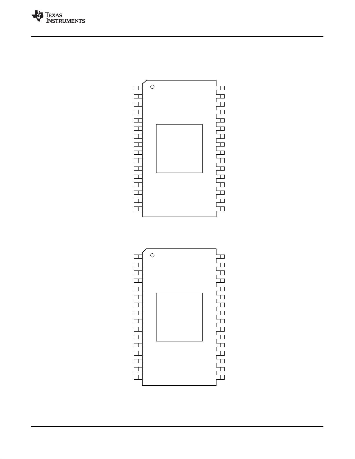
器器件件型型号号 封封装装 封封装装尺尺寸寸((标标称称值值))
• 立体声模式和单声道模式(采用单滤波器单声道配
DAD (32)
置)
TPA3116D2 11.00mm x 6.20mm
DAP (32)
• 由单电源供电运行,减少了元件数量
TPA3118D2
DAP (32) 11.00mm x 6.20mm
• 集成了具有错误报告功能的自保护电路,其中包括
TPA3130D2
过压、欠压、过热、直流检测和短路等保护
(1) 如需了解所有可用封装,请见数据表末尾的可订购产品附录。
• 耐热增强型封装
简简化化应应用用电电路路
– DAD(32 位引脚散热薄型小外形尺寸
(HTSSOP) 封装,焊盘朝上)
– DAP(32 位 HTSSOP 封装,焊盘朝下)
• -40°C 至 85°C 环境温度范围
2 应应用用
• 小型-微型组件、扬声器、扩展坞底座
• 汽车售后
• 阴极射线管 (CRT) TV
• 消费类音频应用
1
PRODUCTION DATA information is current as of publication date. Products conform to specifications per the terms of the Texas
Instruments standard warranty. Production processing does not necessarily include testing of all parameters.
English Data Sheet: SLOS708
TPA3116D2
,
TPA3118D2
,
TPA3130D2
ZHCS891D –APRIL 2012–REVISED JANUARY 2015
www.ti.com.cn
目目录录
7.3 Feature Description................................................. 13
1 特特性性.......................................................................... 1
7.4 Device Functional Modes........................................ 24
2 应应用用.......................................................................... 1
8 Applications and Implementation ...................... 25
3 说说明明.......................................................................... 1
8.1 Application Information............................................ 25
4 修修订订历历史史记记录录 ........................................................... 2
8.2 Typical Application .................................................. 25
5 Pin Configuration and Functions......................... 3
9 Power Supply Recommendations...................... 28
6 Specifications......................................................... 5
10 Layout................................................................... 28
6.1 Absolute Maximum Ratings ...................................... 5
10.1 Layout Guidelines ................................................. 28
6.2 ESD Ratings ............................................................ 5
10.2 Layout Example .................................................... 29
6.3 Recommended Operating Conditions....................... 5
10.3 Heat Sink Used on the EVM ................................. 31
6.4 Thermal Information.................................................. 6
11 器器件件和和文文档档支支持持 ..................................................... 32
6.5 DC Electrical Characteristics .................................... 6
11.1 相关链接................................................................ 32
6.6 AC Electrical Characteristics..................................... 6
11.2 商标 ....................................................................... 32
6.7 Typical Characteristics.............................................. 8
11.3 静电放电警告......................................................... 32
7 Detailed Description............................................ 13
11.4 术语表 ................................................................... 32
7.1 Overview ................................................................. 13
12 机机械械、、封封装装和和可可订订购购信信息息....................................... 32
7.2 Functional Block Diagram ....................................... 13
4 修修订订历历史史记记录录
Changes from Revision C (April 2012) to Revision D Page
• 已添加
引脚配置和功能
部分、ESD
额定值
表、
特性描述
部分、
器件功能模式
、
应用和实施
部分、
电源相关建议
部分、
布局
部分、
器件和文档支持
部分以及
机械、封装和可订购信息
部分........................................................................................ 1
Changes from Revision B (May 2012) to Revision C Page
• Changed Notes 2 and 3 of the Thermal Information Table.................................................................................................... 6
• Changed the Gain (BTL) Test Condition values for R1 and R2............................................................................................. 6
• Changed the Gain (SLV) Test Condition values for R1 and R2............................................................................................. 6
• Changed the SYSTEM BLOCK DIAGRAM .......................................................................................................................... 13
2 Copyright © 2012–2015, Texas Instruments Incorporated
32
31
30
29
19
13
14
15
16
17
18
20
1
2
3
4
5
6
7
8
9
10
11
12 21
22
23
24
28
27
26
25
FAULTZ
SDZ
SYNC
AM0
AM1
MUTE
LINN
LINP
PLIMIT
RINN
GVDD
RINP
AVCC
OUTPR
PVCC
BSPL
GND
OUTPL
PVCC
OUTNL
BSNL
PVCC
OUTNR
BSNR
MODSEL
BSPR
GND
GND
PVCC
GND
GAIN/SLV
AM2
Thermal
PAD
32
31
30
29
19
13
14
15
16
17
18
20
1
2
3
4
5
6
7
8
9
10
11
12 21
22
23
24
28
27
26
25
FAULTZ
SDZ
SYNC
AM0
AM1
MUTE
LINN
LINP
PLIMIT
RINN
GVDD
RINP
AVCC
OUTPR
PVCC
BSPL
GND
OUTPL
PVCC
OUTNL
BSNL
PVCC
OUTNR
BSNR
MODSEL
BSPR
GND
GND
PVCC
GND
GAIN/SLV
AM2
Thermal
PAD
TPA3116D2
,
TPA3118D2
,
TPA3130D2
www.ti.com.cn
ZHCS891D –APRIL 2012–REVISED JANUARY 2015
5 Pin Configuration and Functions
DAD Package
32-Pin HTSSOP With PowerPAD Up
TPA3116D2 Only, Top View
DAP Package
32-Pin HTSSOP With PowerPAD Down
Top View
Copyright © 2012–2015, Texas Instruments Incorporated 3
TPA3116D2
,
TPA3118D2
,
TPA3130D2
ZHCS891D –APRIL 2012–REVISED JANUARY 2015
www.ti.com.cn
Pin Functions
PIN
TYPE
(1)
DESCRIPTION
NO. NAME
1 MODSEL I Mode selection logic input (LOW = BD mode, HIGH = 1 SPW mode). TTL logic levels with compliance to
AVCC.
2 SDZ I Shutdown logic input for audio amp (LOW = outputs Hi-Z, HIGH = outputs enabled). TTL logic levels with
compliance to AVCC.
3 FAULTZ DO General fault reporting including Over-temp, DC Detect. Open drain.
FAULTZ = High, normal operation
FAULTZ = Low, fault condition
4 RINP I Positive audio input for right channel. Biased at 3 V.
5 RINN I Negative audio input for right channel. Biased at 3 V.
6 PLIMIT I Power limit level adjust. Connect a resistor divider from GVDD to GND to set power limit. Connect directly
to GVDD for no power limit.
7 GVDD PO Internally generated gate voltage supply. Not to be used as a supply or connected to any component other
than a 1 µF X7R ceramic decoupling capacitor and the PLIMIT and GAIN/SLV resistor dividers.
8 GAIN/SLV I Selects Gain and selects between Master and Slave mode depending on pin voltage divider.
9 GND G Ground
10 LINP I Positive audio input for left channel. Biased at 3 V. Connect to GND for PBTL mode.
11 LINN I Negative audio input for left channel. Biased at 3 V. Connect to GND for PBTL mode.
12 MUTE I Mute signal for fast disable/enable of outputs (HIGH = outputs Hi-Z, LOW = outputs enabled). TTL logic
levels with compliance to AVCC.
13 AM2 I AM Avoidance Frequency Selection
14 AM1 I AM Avoidance Frequency Selection
15 AM0 I AM Avoidance Frequency Selection
16 SYNC DIO Clock input/output for synchronizing multiple class-D devices. Direction determined by GAIN/SLV terminal.
17 AVCC P Analog Supply
18 PVCC P Power supply
19 PVCC P Power supply
20 BSNL BST Boot strap for negative left channel output, connect to 220 nF X5R, or better ceramic cap to OUTPL
21 OUTNL PO Negative left channel output
22 GND G Ground
23 OUTPL PO Positive left channel output
24 BSPL BST Boot strap for positive left channel output, connect to 220 nF X5R, or better ceramic cap to OUTNL
25 GND G Ground
26 BSNR BST Boot strap for negative right channel output, connect to 220 nF X5R, or better ceramic cap to OUTNR
27 OUTNR PO Negative right channel output
28 GND G Ground
29 OUTPR PO Positive right channel output
30 BSPR BST Boot strap for positive right channel output, connect to 220 nF X5R or better ceramic cap to OUTPR
31 PVCC P Power supply
32 PVCC P Power supply
33 PowerPAD G Connect to GND for best system performance. If not connected to GND, leave floating.
(1) TYPE: DO = Digital Output, I = Analog Input, G = General Ground, PO = Power Output, BST = Boot Strap.
4 Copyright © 2012–2015, Texas Instruments Incorporated
TPA3116D2
,
TPA3118D2
,
TPA3130D2
www.ti.com.cn
ZHCS891D –APRIL 2012–REVISED JANUARY 2015
6 Specifications
6.1 Absolute Maximum Ratings
over operating free-air temperature range (unless otherwise noted)
(1)
MIN MAX UNIT
Supply voltage, V
CC
PV
CC
, AV
CC
–0.3 30 V
INPL, INNL, INPR, INNR –0.3 6.3 V
Input voltage, V
I
PLIMIT, GAIN / SLV, SYNC –0.3 GVDD+0.3 V
AM0, AM1, AM2, MUTE, SDZ, MODSEL –0.3 PVCC+0.3 V
Slew rate, maximum
(2)
AM0, AM1, AM2, MUTE, SDZ, MODSEL 10 V/ms
Operating free-air temperature, T
A
–40 85 °C
Operating junction temperature , T
J
–40 150 °C
Storage temperature, T
stg
–40 125 °C
(1) Stresses beyond those listed under absolute maximum ratings may cause permanent damage to the device. These are stress ratings
only, and functional operation of the device at these or any other conditions beyond those indicated under recommended operating
conditions is not implied. Exposure to absolute-maximum-rated conditions for extended periods may affect device reliability.
(2) 100 kΩ series resistor is needed if maximum slew rate is exceeded.
6.2 ESD Ratings
VALUE UNIT
Human-body model (HBM), per ANSI/ESDA/JEDEC JS-001
(1)
±2000
V
(ESD)
Electrostatic discharge V
Charged-device model (CDM), per JEDEC specification JESD22- ±500
C101
(2)
(1) JEDEC document JEP155 states that 500-V HBM allows safe manufacturing with a standard ESD control process.
(2) JEDEC document JEP157 states that 250-V CDM allows safe manufacturing with a standard ESD control process. .
6.3 Recommended Operating Conditions
over operating free-air temperature range (unless otherwise noted)
MIN NOM MAX UNIT
V
CC
Supply voltage PV
CC
, AV
CC
4.5 26 V
High-level input
V
IH
AM0, AM1, AM2, MUTE, SDZ, SYNC, MODSEL 2 V
voltage
Low-level input
V
IL
AM0, AM1, AM2, MUTE, SDZ, SYNC, MODSEL 0.8 V
voltage
Low-level output
V
OL
FAULTZ, R
PULL-UP
= 100 kΩ, PV
CC
= 26 V 0.8 V
voltage
High-level input
I
IH
AM0, AM1, AM2, MUTE, SDZ, MODSEL (V
I
= 2 V, V
CC
= 18 V) 50 µA
current
TPA3116D2, TPA3118D2 3.2 4
R
L
(BTL) Output filter: L = 10 µH, C = 680 nF
TPA3130D2 5.6 8
Minimum load
Ω
Impedance
TPA3116D2, TPA3118D2 1.6
R
L
(PBTL) Output filter: L = 10 µH, C = 1 µF
TPA3130D2 3.2 4
Output-filter
L
o
Minimum output filter inductance under short-circuit condition 1 µH
Inductance
Copyright © 2012–2015, Texas Instruments Incorporated 5
剩余41页未读,继续阅读
电傻了
- 粉丝: 0
- 资源: 3
上传资源 快速赚钱
- 我的内容管理 收起
- 我的资源 快来上传第一个资源
- 我的收益 登录查看自己的收益
- 我的积分 登录查看自己的积分
- 我的C币 登录后查看C币余额
- 我的收藏
- 我的下载
- 下载帮助
会员权益专享
最新资源
- zigbee-cluster-library-specification
- JSBSim Reference Manual
- c++校园超市商品信息管理系统课程设计说明书(含源代码) (2).pdf
- 建筑供配电系统相关课件.pptx
- 企业管理规章制度及管理模式.doc
- vb打开摄像头.doc
- 云计算-可信计算中认证协议改进方案.pdf
- [详细完整版]单片机编程4.ppt
- c语言常用算法.pdf
- c++经典程序代码大全.pdf
- 单片机数字时钟资料.doc
- 11项目管理前沿1.0.pptx
- 基于ssm的“魅力”繁峙宣传网站的设计与实现论文.doc
- 智慧交通综合解决方案.pptx
- 建筑防潮设计-PowerPointPresentati.pptx
- SPC统计过程控制程序.pptx
资源上传下载、课程学习等过程中有任何疑问或建议,欢迎提出宝贵意见哦~我们会及时处理!
点击此处反馈
安全验证
文档复制为VIP权益,开通VIP直接复制
信息提交成功
评论1