TI OPA847:3.9GHz带宽低噪声运算放大器
需积分: 50 122 浏览量
更新于2023-06-03
收藏 884KB PDF 举报
"OPA847是一款由TI公司推出的高性能运算放大器,以其超宽带宽、极低噪声和高增益带宽比等特点而著称。这款运放适用于多种应用,包括高动态范围ADC前置放大器、低噪声宽频带跨阻放大器、宽频带高增益放大器、低噪声差分接收器、超声波通道放大器以及OPA687、CLC425和LMH6624等产品的升级选项。OPA847的主要特性包括:3.9GHz的高增益带宽、0.85nV/√Hz的低输入电压噪声、-105dBc的低失真(在5MHz时)、950V/μs的高速上升率、±100μV以下的高直流精度、18.1mA的低供电电流以及2mW的关断功率。此外,该运放还具有一个可选的电源关闭引脚,当拉低该引脚时,可以将放大器的供电电流降低到正常工作状态的1%以下,从而实现节能。"
OPA847运算放大器在设计上兼顾了高性能与低功耗,使其在各种对噪声和速度有严苛要求的应用中表现出色。其3.9GHz的增益带宽产品意味着它可以处理非常高的频率信号,适合于需要快速响应的系统。0.85nV/√Hz的输入电压噪声则表明OPA847在噪声性能上极其出色,这对于要求极高信噪比的信号放大应用至关重要。此外,-105dBc的失真度在5MHz时仍然保持很低,这确保了放大信号的线性度,对于音频和测量设备等需要低失真的应用来说是理想选择。
950V/μs的上升速率使得OPA847能够快速响应瞬态信号,这对于高速数据采集系统和高频信号处理应用至关重要。高直流精度保证了在放大直流信号时的稳定性和准确性,这在精确测量和控制电路中非常重要。18.1mA的低供电电流则意味着OPA847可以在保持高性能的同时,降低系统的整体能耗。
电源关闭功能是OPA847的一个独特之处,它允许在不需要放大器工作时将其关闭,以进一步节省电力。这种特性在电池供电或能源有限的系统中非常有用,如远程传感器和便携式设备。当不需要电源关闭功能时,只需断开电源关闭引脚即可保证正常运行。
OPA847是一款高性能、低噪声、高带宽的运算放大器,适用于对信号质量和速度有极高要求的领域,如高端音频设备、医疗成像系统、航空航天电子、射频通信和精密测量仪器等。它的设计考虑了低功耗的需求,使其成为各种应用的理想选择,尤其是那些需要在性能和能效之间取得平衡的场合。
OPA847
6
SBOS251E
www.ti.com
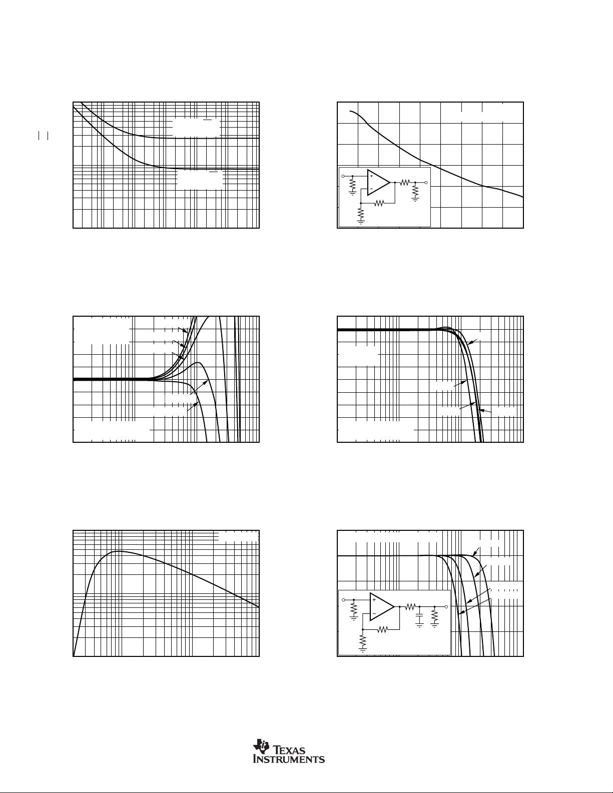
TYPICAL CHARACTERISTICS: V
S
= ±5V (Cont.)
T
A
= 25°C, G = +20V/V, R
G
= 39.2Ω, and R
L
= 100Ω, unless otherwise noted.
10
1
0
INPUT VOLTAGE AND CURRENT NOISE
Frequency (Hz)
Voltage Noise (nV/√Hz)
Current Voise (pA/√Hz)
10
1
10
2
10
3
10
4
10
5
10
6
10
7
2.7pA/√Hz
Current Noise
0.85nV/√Hz
Voltage Noise
50
45
40
35
30
25
20
2-TONE, 3RD-ORDER INTERMODULATION INTERCEPT
Frequency (MHz)
Intercept Point (+dBm)
5101520253035404550
G = +20V/V
20dB to matched load.
750Ω
50Ω
OPA847
P
I
P
O
50Ω
50Ω
39.2Ω
0.5
0.4
0.3
0.2
0.1
0
–0.1
–0.2
–0.3
–0.4
–0.5
NONINVERTING GAIN FLATNESS TUNE
Frequency (MHz)
Deviation from 21.58dB Gain (0.1dB)
1 10 100 1000
NG = 12
NG = 14
NG = 20
NG = 18
NG = 16
V
O
= 200mV
PP
A
V
= +12V/V
NG = Noise Gain
External Compensation
See Figure 8
1
0
–1
–2
–3
–4
–5
–6
–7
–8
–9
LOW GAIN INVERTING BANDWIDTH
Frequency (MHz)
Normalized Gain (1dB)
1 10 100 1000
G = –8
G = –4
G = –2
G = –1
V
O
= 0.2V
PP
R
F
= 750Ω
External Compensation
See Figure 6
100
10
1
RECOMMENDED R
S
vs CAPACITIVE LOAD
Capacitive Load (pF)
R
S
(Ω)
1 10 100 1000
G = +20V/V
29
26
23
20
17
14
FREQUENCY RESPONSE vs CAPACITIVE LOAD
Frequency (MHz)
Normalized Gain to Capacitive Load (dB)
1 10 100 1000
C = 22pF
C = 47pF
C = 100pF
C = 10pF
R
S
adjusted for capacitive load.
750Ω
R
S
OPA847
V
I
V
O
50Ω
1kΩ
C
L
39.2Ω
(1kΩ is optional.)
剩余29页未读,继续阅读
2016-04-18 上传
2014-08-22 上传
2020-07-27 上传
点击了解资源详情
点击了解资源详情
点击了解资源详情

Yuan-T
- 粉丝: 1
- 资源: 2
 我的内容管理
展开
我的内容管理
展开


最新资源
- SSM动力电池数据管理系统源码及数据库详解
- R语言桑基图绘制与SCI图输入文件代码分析
- Linux下Sakagari Hurricane翻译工作:cpktools的使用教程
- prettybench: 让 Go 基准测试结果更易读
- Python官方文档查询库,提升开发效率与时间节约
- 基于Django的Python就业系统毕设源码
- 高并发下的SpringBoot与Nginx+Redis会话共享解决方案
- 构建问答游戏:Node.js与Express.js实战教程
- MATLAB在旅行商问题中的应用与优化方法研究
- OMAPL138 DSP平台UPP接口编程实践
- 杰克逊维尔非营利地基工程的VMS项目介绍
- 宠物猫企业网站模板PHP源码下载
- 52简易计算器源码解析与下载指南
- 探索Node.js v6.2.1 - 事件驱动的高性能Web服务器环境
- 找回WinSCP密码的神器:winscppasswd工具介绍
- xctools:解析Xcode命令行工具输出的Ruby库
