没有合适的资源?快使用搜索试试~ 我知道了~
首页差分放大器INA128
资源详情
资源评论
资源推荐
FEATURES
D LOW OFFSET VOLTAGE: 50µV max
D LOW DRIFT: 0.5µV/5C max
D LOW INPUT BIAS CURRENT: 5nA max
D HIGH CMR: 120dB min
D INPUTS PROTECTED TO +40V
D WIDE SUPPLY RANGE: +2.25V to +18V
D LOW QUIESCENT CURRENT: 700µA
D 8-PIN PLASTIC DIP, SO-8
APPLICATIONS
D BRIDGE AMPLIFIER
D THERMOCOUPLE AMPLIFIER
D RTD SENSOR AMPLIFIER
D MEDICAL INSTRUMENTATION
D DATA ACQUISITION
DESCRIPTION
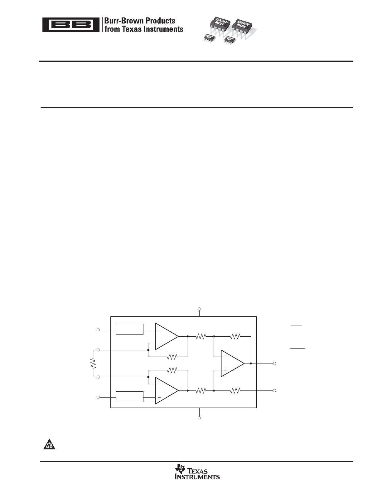
The INA128 and INA129 are low power, general
purpose instrumentation amplifiers offering excellent
accuracy. The versatile 3-op amp design and small size
make them ideal for a wide range of applications.
Current-feedback input circuitry provides wide
bandwidth even at high gain (200kHz at G = 100).
A single external resistor sets any gain from 1 to 10,000.
The INA128 provides an industry-standard gain
equation; the INA129 gain equation is compatible with
the AD620.
The INA128/INA129 is laser trimmed for very low offset
voltage (50µV), drift (0.5µV/°C) and high
common-mode rejection (120dB at G ≥ 100). It
operates with power supplies as low as ±2.25V, and
quiescent current is only 700µA—ideal for battery-
operated systems. Internal input protection can
withstand up to ±40V without damage.
The INA128/INA129 is available in 8-pin plastic DIP and
SO-8 surface-mount packages, specified for the –40°C
to +85°C temperature range. The INA128 is also
available in a dual configuration, the INA2128.
A
1
A
2
A
3
40k
Ω
40k
Ω
40k
Ω
40k
Ω
V
IN
2
1
8
3
6
5
V
IN
R
G
V+
V
−
Ref
V
O
G=1+
49.4k
Ω
R
G
−
+
4
7
NOTE: (1) INA129: 24.7k
Ω
G=1+
50k
Ω
R
G
INA128, INA129
Over-Voltage
Protection
Over-Voltage
Protection
25kΩ
(1)
25kΩ
(1)
INA128:
INA129:
All trademarks are the property of their respective owners.
INA128
INA129
Precision, Low Power
INSTRUMENTATION AMPLIFIERS
SBOS051B − OCTOBER 1995 − REVISED FEBRUARY 2005
! !
www.ti.com
Copyright 1995−2005, Texas Instruments Incorporated
Please be aware that an important notice concerning availability, standard warranty, and use in critical applications of Texas Instruments
semiconductor products and disclaimers thereto appears at the end of this data sheet.
"#$
"#%
SBOS051B − OCTOBER 1995 − REVISED FEBRUARY 2005
www.ti.com
2
ABSOLUTE MAXIMUM RATINGS
(1)
Supply Voltage ±18V. . . . . . . . . . . . . . . . . . . . . . . . . . . . . . . . . . . . . .
Analog Input Voltage Range ±40V. . . . . . . . . . . . . . . . . . . . . . . . . . .
Output Short-Circuit (to ground) Continuous. . . . . . . . . . . . . . . . . .
Operating Temperature −40°C to +125°C. . . . . . . . . . . . . . . . . . .
Storage Temperature Range −55°C to +125°C. . . . . . . . . . . . . . . . .
Junction Temperature +150°C. . . . . . . . . . . . . . . . . . . . . . . . . . . . . . .
Lead Temperature (soldering, 10s) +300°C. . . . . . . . . . . . . . . . . . . . .
(1)
Stresses above these ratings may cause permanent damage.
Exposure to absolute maximum conditions for extended periods
may degrade device reliability. These are stress ratings only, and
functional operation of the device at these or any other conditions
beyond those specified is not implied.
ELECTROSTATIC DISCHARGE SENSITIVITY
This integrated circuit can be damaged by
ESD. Texas Instruments recommends that all
integrated circuits be handled with appropriate
precautions. Failure to observe proper handling and
installation procedures can cause damage.
ESD damage can range from subtle performance
degradation to complete device failure. Precision
integrated circuits may be more susceptible to damage
because very small parametric changes could cause the
device not to meet its published specifications.
ORDERING INFORMATION
For the most current package and ordering information, see the Package Option Addendum located at the end of this data
sheet.
PIN CONFIGURATION
R
G
V
−
IN
V
+
IN
V−
R
G
V+
V
O
Ref
1
2
3
4
8
7
6
5
Top View
8-Pin DIP and SO-8
"#$
"#%
SBOS051B − OCTOBER 1995 − REVISED FEBRUARY 2005
www.ti.com
3
ELECTRICAL CHARACTERISTICS
At T
A
= +25°C, V
S
= ±15V, R
L
= 10kΩ, unless otherwise noted.
INA128P, U
INA129P. U
INA128PA, UA
INA129PA, UA
PARAMETER CONDITIONS MIN TYP MAX MIN TYP MAX UNIT
INPUT
Offset Voltage, RTI
Initial T
A
= +25°C ±10±100/G ±50±500/G ±25±100/G ±125±1000/G µV
vs Temperature T
A
= T
MIN
to T
MAX
±0.2±2/G ±0.5±20/G ±0.2±5/G ±1±20/G µV/°C
vs Power Supply V
S
= ±2.25V to ±18V ±0.2±20/G ±1±100/G ∗ ±2±200/G µV/V
Long-Term Stability ±0.1±3/G ∗ µV/mo
Impedance, Differential 10
10
|| 2 ∗ Ω || pF
Common-Mode 10
11
|| 9 ∗ Ω || pF
Common-Mode Voltage Range
(1)
V
O
= 0V (V+) − 2 (V+) − 1.4 ∗ ∗ V
(V−) + 2 (V−) + 1.7 ∗ ∗ V
Safe Input Voltage ±40 ∗ V
Common-Mode Rejection V
CM
= ±13V, ∆R
S
= 1kΩ
G = 1 80 86 73 ∗ dB
G = 10 100 106 93 ∗ dB
G = 100 120 125 110 ∗ dB
G = 1000 120 130 110 ∗ dB
BIAS CURRENT ±2 ±5 ∗ ±10 nA
vs Temperature ±30 ∗ pA/°C
Offset Current ±1 ±5 ∗ ±10 nA
vs Temperature ±30 ∗ pA/°C
NOISE VOLTAGE, RTI G = 1000, R
S
= 0Ω
f = 10Hz 10 ∗ nV/√Hz
f = 100Hz 8 ∗ nV/√Hz
f = 1kHz 8 ∗ nV/√Hz
f
B
= 0.1Hz to 10Hz 0.2 ∗ µV
PP
Noise Current
f = 10Hz 0.9 ∗ pA/√Hz
f = 1kHz 0.3 ∗ pA/√Hz
f
B
= 0.1Hz to 10Hz 30 ∗ pA
PP
GAIN
Gain Equation, INA128 1 + (50kΩ/R
G
) ∗ V/V
Gain Equation, INA129 1 + (49.4kΩ/R
G
) ∗ V/V
Range of Gain 1 10000 ∗ ∗ V/V
Gain Error G = 1 ±0.01 ±0.024 ∗ ±0.1 %
G = 10 ±0.02 ±0.4 ∗ ±0.5 %
G = 100 ±0.05 ±0.5 ∗ ±0.7 %
G = 1000 ±0.5 ±1 ∗ ±2 %
Gain vs Temperature
(2)
G = 1 ±1 ±10 ∗ ∗ ppm/°C
50kΩ (or 49.4kΩ) Resistance
(2)(3)
±25 ±100 ∗ ∗ ppm/°C
Nonlinearity V
O
= ±13.6V, G = 1 ±0.0001 ±0.001 ∗ ±0.002 % of FSR
G = 10 ±0.0003 ±0.002 ∗ ±0.004 % of FSR
G = 100 ±0.0005 ±0.002 ∗ ±0.004 % of FSR
G = 1000 ±0.001
(4)
∗ ∗ % of FSR
NOTE
:
∗ Specification is same as INA128P, U or INA129P, U.
(1)
Input common-mode range varies with output voltage — see typical curves.
(2)
Specified by wafer test.
(3)
Temperature coefficient of the 50kΩ (or 49.4kΩ) term in the gain equation.
(4)
Nonlinearity measurements in G = 1000 are dominated by noise. Typical nonlinearity is ±0.001%.
"#$
"#%
SBOS051B − OCTOBER 1995 − REVISED FEBRUARY 2005
www.ti.com
4
ELECTRICAL CHARACTERISTICS (continued)
At T
A
= +25°C, V
S
= ±15V, R
L
= 10kΩ, unless otherwise noted.
INA128PA, UA
INA129PA, UA
INA128P, U
INA129P. U
PARAMETER UNITMAXTYPMINMAXTYPMINCONDITIONS
OUTPUT
Voltage: Positive R
L
= 10kΩ (V+) − 1.4 (V+) − 0.9 ∗ ∗ V
Voltage: Negative R
L
= 10kΩ (V−) + 1.4 (V−) + 0.8 ∗ ∗ V
Load Capacitance Stability 1000 ∗ pF
Short-Circuit Current +6/−15 ∗ mA
FREQUENCY RESPONSE
Bandwidth, −3dB G = 1 1.3 ∗ MHz
G = 10 700 ∗ kHz
G = 100 200 ∗ kHz
G = 1000 20 ∗ kHz
Slew Rate V
O
= ±10V, G = 10 4 ∗ V/µs
Settling Time, 0.01% G = 1 7 ∗ µs
G = 10 7 ∗ µs
G = 100 9 ∗ µs
G = 1000 80 ∗ µs
Overload Recovery 50% Overdrive 4 ∗ µs
POWER SUPPLY
Voltage Range ±2.25 ±15 ±18 ∗ ∗ ∗ V
Current, Total V
IN
= 0V ±700 ±750 ∗ ∗ µA
TEMPERATURE RANGE
Specification −40 +85 ∗ ∗ °C
Operating −40 +125 ∗ ∗ °C
q
JA
8-Pin DIP 80 ∗ °C/W
SO-8 SOIC 150 ∗ °C/W
NOTE
:
∗ Specification is same as INA128P, U or INA129P, U.
(1)
Input common-mode range varies with output voltage — see typical curves.
(2)
Specified by wafer test.
(3)
Temperature coefficient of the 50kΩ (or 49.4kΩ) term in the gain equation.
(4)
Nonlinearity measurements in G = 1000 are dominated by noise. Typical nonlinearity is ±0.001%.
剩余17页未读,继续阅读
米斯特杨_666
- 粉丝: 1
- 资源: 2
上传资源 快速赚钱
- 我的内容管理 收起
- 我的资源 快来上传第一个资源
- 我的收益 登录查看自己的收益
- 我的积分 登录查看自己的积分
- 我的C币 登录后查看C币余额
- 我的收藏
- 我的下载
- 下载帮助
会员权益专享
最新资源
- zigbee-cluster-library-specification
- JSBSim Reference Manual
- c++校园超市商品信息管理系统课程设计说明书(含源代码) (2).pdf
- 建筑供配电系统相关课件.pptx
- 企业管理规章制度及管理模式.doc
- vb打开摄像头.doc
- 云计算-可信计算中认证协议改进方案.pdf
- [详细完整版]单片机编程4.ppt
- c语言常用算法.pdf
- c++经典程序代码大全.pdf
- 单片机数字时钟资料.doc
- 11项目管理前沿1.0.pptx
- 基于ssm的“魅力”繁峙宣传网站的设计与实现论文.doc
- 智慧交通综合解决方案.pptx
- 建筑防潮设计-PowerPointPresentati.pptx
- SPC统计过程控制程序.pptx
资源上传下载、课程学习等过程中有任何疑问或建议,欢迎提出宝贵意见哦~我们会及时处理!
点击此处反馈
安全验证
文档复制为VIP权益,开通VIP直接复制
信息提交成功
评论0