没有合适的资源?快使用搜索试试~ 我知道了~
首页A3P1000 FPGA 说明
资源详情
资源评论
资源推荐
August 2012 1
Migrating Designs in ProASIC3 Devices from
Higher-Density to Mid-Density Devices
Introduction
The purpose of this document is to assist in migrating designs in ProASIC
®
3 A3P1000, A3P600, and
A3P400 devices from higher-density to mid-density devices. There are three possible migration paths:
• A3P1000 to A3P600
• A3P1000 to A3P400
• A3P600 to A3P400
Since one of the key factors is pin compatibility, this document addresses pin compatibility for all
available packages common to the A3P1000, A3P600, and A3P400 devices.
Design Migration
ProASIC3 family devices are architecturally compatible with each other. However, designers must pay
attention to a few key areas when migrating a design. The specific issues discussed throughout this
application note are as follows:
• "Design and Device Evaluation"
• "Device and Package Compatibility" on page 2
• "Migration and Implementation Methodologies" on page 3
• "I/O Banks and Standards" on page 4
• "Power Supply and Board-Level Considerations" on page 4
• "Pin Migration and Compatibility" on page 5
Design and Device Evaluation
When migrating a design, the primary task should be to compare the available resources between the
two devices. The designer should evaluate effective gate count, RAM size, I/O banks, and number of
I/Os (Table 1). In addition, necessary design timing analysis and simulations should be validated when
porting designs to new ProASIC3 derivatives.
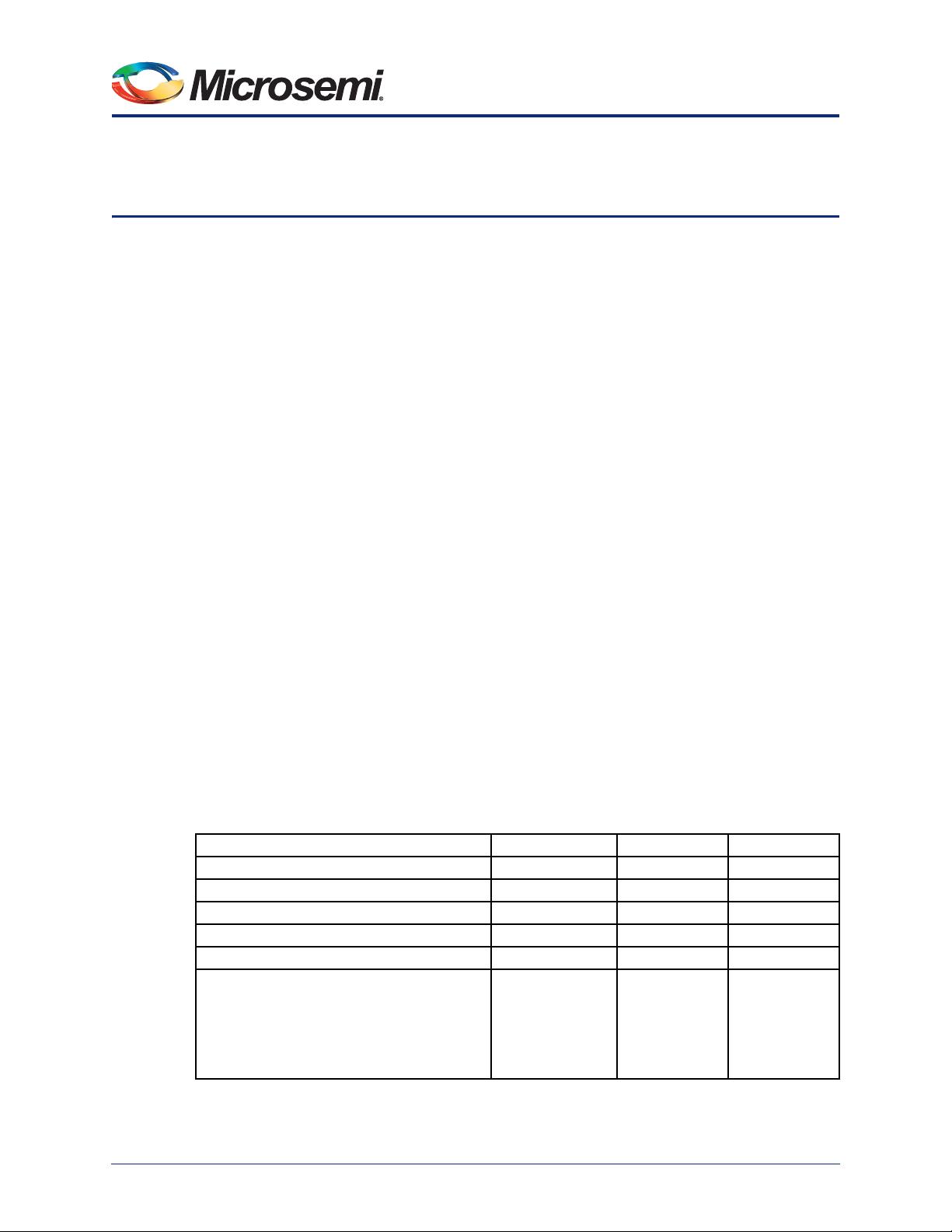
Table 1 • Device Information
A3P1000 A3P600 A3P400
System Gates 1 M 600 k 400 k
Tiles (D-flip-flop) 24,576 13,824 9,126
RAM (kbits) 144 108 54
RAM Blocks (4,608 bits) 32 24 12
I/O Banks (+ JTAG) 444
Maximum User I/Os per Package
PQ208
FG144
FG256
FG484
154/35
97/25
177/44
300/74
154/35
97/25
177/43
235/60
151/34
97/25
178/38
194/38
Note: Maximum user I/O is listed as single-ended/double-ended.
Device and Package Compatibility
2 August 2012
Device and Package Compatibility
ProASIC3 devices and packaging were designed to allow considerable footprint compatibility for
smoother migration.
Common and Convertible I/Os between A3P400, A3P600, and
A3P1000 Devices
Table 2 shows the number of I/Os that are common between any two of these devices, as well as the
number of I/Os that will require conversion per the suggested design migration rules given in the
"Migration and Implementation Methodologies" section on page 3.
Table 2 • Common and Convertible I/Os
Package
A3P1000
A3P600
A3P1000
A3P400
A3P600
A3P400
Common
I/Os
Convertible
I/Os
Common
I/Os
Convertible
I/Os
Common
I/Os
Convertible
I/Os
PQ208 154015451515
FG144 970970980
FG256 178311775917733
FG484 236 96 192 75 236 166
Migrating Designs in ProASIC3 Devices from Higher-Density to Mid-Density Devices
August 2012 3
Migration and Implementation Methodologies
Table 3 lists some possible migration combinations and the recommended implementation rules for
compatible design conversions from higher-density to lower-density devices. The "Pin Migration and
Compatibility" section on page 5 contains tables that list the required rules for different pin combinations.
If “Rule x” is mentioned for a pin combination, that combination requires the implementation methodology
given in Table 3. Note that many combinations of high-density/low-density pins do not require these
rules; the pins have complete type compatibility. These pins are marked in the pin tables with “None.”
Table 3 • Migration Rules from Higher-Density to Mid-Density Devices
Migration
Rule
Issue
Implementation MethodologyHigher Density Lower Density
1 I/O or global I/O NC Leave this pin floating OR program I/Os as unused (software
cannot program NC to usable I/O).
2 Single-ended I/O Global I/O Instantiate the I/O buffer as a global single-ended I/O.
3 Global I/O Single-ended I/O Use the physical design constraint (PDC) to promote the
single-ended I/O to a global pin. There is an additional delay
that affects the setup time on the board. Or, do not use this
pin as a global input on the higher-density device.
4 VCC or VCCIB(x)
1,3
NC Leave pin connected to board VCC or VCCIBx plane.
5 VCCIB(x)
1
VCCIB(y)
2
Make sure the two bank voltage levels are the same. Tie the
pin to the board’s corresponding VCCIBx/VMVx plane.
6 VMV(x)
1
VMV(y)
2
Make sure the two bank voltage levels are the same. Tie pin
to the board’s corresponding VCCIBx/VMVx plane.
7 VMV(x)
2
I/O or global I/O Leave the pin tied to the board VCCIBx/VMVx plane.
Instantiate the I/Os as tristate buffers with OE = 0 and no
weak pull-ups/-downs.
8 GNDQ Global I/O Leave both pins tied to board GNDQ plane. Instantiate the
I/O as tristate buffer with OE = 0 and no weak pull-ups/-
downs.
9 GNDQ NC GNDQ and NC need to be connected to GND.
10 NC VCC or VCCIB(x)
1,3
Leave pin connected to board VCC or VCCIBx plane.
Notes:
1. (x) = 1, 2, 3, or 4
2. (y) = 1, 2, 3, or 4
3. Refer to the "I/O Structures in IGLOO and ProASIC3 Devices" chapter of the IGLOO FPGA Fabric User’s Guide
or ProASIC3 FPGA Fabric User’s Guide for I/O naming conventions.
I/O Banks and Standards
4 August 2012
I/O Banks and Standards
ProASIC3 I/Os are partitioned into multiple I/O voltage banks. The number of banks is device-dependent.
There are four I/O banks in A3P1000, A3P600, and A3P400 devices.
Package VCCIBx pins are routed through the corresponding banks of the devices.
The banks have dedicated supplies; therefore, only I/Os with compatible voltage standards can be
assigned to the same I/O voltage bank.
Power Supply and Board-Level Considerations
I/O power supply requirements are one of the key aspects to consider for design migration. Since the
migration is within the ProASIC3 family, there is no issue with respect to the core voltage, VCC. Pins that
must be appropriately connected are VCCIBx (bank supply voltage to I/O output buffer and I/O logic),
VMVx (quiet I/O supply voltage), GNDQ (quiet GND), and GND. An important function of GNDQ and
VMVx is to decouple simultaneous switching noise for outputs (SSOs) to enhance signal integrity and
improve noise immunity.
The following are the key rules of migration for the above-mentioned pins:
• VMVx and VCCIBx must be at the same voltage level for a given bank.
• VCCIBx pins and VMVx pins in unused banks must be connected to GND.
• Unused I/Os are automatically disabled by software.
A specific power-supply sequence at power-up is not required.
Any incorrect connection during the migration may affect overall dynamic or inrush power consumption
and might even result in device malfunction.
Additionally, the I/O naming convention in ProASIC3 devices has significant embedded information (i.e.,
pin location, bank number, signal type, polarity, and clock conditioning). For a detailed explanation, refer
to the “User I/O Naming Convention” section in the "I/O Structures in IGLOO and ProASIC3 Devices"
chapter of the IGLOO FPGA Fabric User’s Guide or ProASIC3 FPGA Fabric User’s Guide. This
datasheet also contains additional information on power issues.
Migrating Designs in ProASIC3 Devices from Higher-Density to Mid-Density Devices
August 2012 5
Pin Migration and Compatibility
PQ208 Package
Table 4 • Pin Compatibility and Migration Table for the PQ208 Package
Pin
Number
A3P1000
Function
A3P600
Function
A3P400
Function
Migration
Rule
between
A3P1000
and
A3P600
Migration
Rule
between
A3P1000
and
A3P400
Migration
Rule
between
A3P600
and
A3P400
1 GND GND GND None None None
2 GAA2/IO225PDB3 GAA2/IO170PDB3 GAA2/IO155UDB3 None None None
3 IO225NDB3 IO170NDB3 IO155VDB3 None None None
4 GAB2/IO224PDB3 GAB2/IO169PDB3 GAB2/IO154UDB3 None None None
5 IO224NDB3 IO169NDB3 IO154VDB3 None None None
6 GAC2/IO223PDB3 GAC2/IO168PDB3 GAC2/IO153UDB3 None None None
7 IO223NDB3 IO168NDB3 IO153VDB3 None None None
8 IO222PDB3 IO167PDB3 IO152UDB3 None None None
9 IO222NDB3 IO167NDB3 IO152VDB3 None None None
10 IO220PDB3 IO166PDB3 IO151UDB3 None None None
11 IO220NDB3 IO166NDB3 IO151VDB3 None None None
12 IO218PDB3 IO165PDB3 IO150PDB3 None None None
13 IO218NDB3 IO165NDB3 IO150NDB3 None None None
14 IO216PDB3 IO164PDB3 IO149PDB3 None None None
15 IO216NDB3 IO164NDB3 IO149NDB3 None None None
16 VCC VCC VCC None None None
17 GND GND GND None None None
18 VCCIB3 VCCIB3 VCCIB3 None None None
19 IO212PDB3 IO163PDB3 IO148PDB3 None None None
20 IO212NDB3 IO163NDB3 IO148NDB3 None None None
21 GFC1/IO209PDB3 GFC1/IO161PDB3 GFC1/IO147PDB3 None None None
22 GFC0/IO209NDB3 GFC0/IO161NDB3 GFC0/IO147NDB3 None None None
23 GFB1/IO208PDB3 GFB1/IO160PDB3 GFB1/IO146PDB3 None None None
24 GFB0/IO208NDB3 GFB0/IO160NDB3 GFB0/IO146NDB3 None None None
25 VCOMPLF VCOMPLF VCOMPLF None None None
26 GFA0/IO207NPB3 GFA0/IO159NPB3 GFA0/IO145NPB3 None None None
27 VCCPLF VCCPLF VCCPLF None None None
28 GFA1/IO207PPB3 GFA1/IO159PPB3 GFA1/IO145PPB3 None None None
29 GND GND GND None None None
剩余40页未读,继续阅读
35617547
- 粉丝: 0
- 资源: 1
上传资源 快速赚钱
- 我的内容管理 收起
- 我的资源 快来上传第一个资源
- 我的收益 登录查看自己的收益
- 我的积分 登录查看自己的积分
- 我的C币 登录后查看C币余额
- 我的收藏
- 我的下载
- 下载帮助
会员权益专享
最新资源
- zigbee-cluster-library-specification
- JSBSim Reference Manual
- c++校园超市商品信息管理系统课程设计说明书(含源代码) (2).pdf
- 建筑供配电系统相关课件.pptx
- 企业管理规章制度及管理模式.doc
- vb打开摄像头.doc
- 云计算-可信计算中认证协议改进方案.pdf
- [详细完整版]单片机编程4.ppt
- c语言常用算法.pdf
- c++经典程序代码大全.pdf
- 单片机数字时钟资料.doc
- 11项目管理前沿1.0.pptx
- 基于ssm的“魅力”繁峙宣传网站的设计与实现论文.doc
- 智慧交通综合解决方案.pptx
- 建筑防潮设计-PowerPointPresentati.pptx
- SPC统计过程控制程序.pptx
资源上传下载、课程学习等过程中有任何疑问或建议,欢迎提出宝贵意见哦~我们会及时处理!
点击此处反馈
安全验证
文档复制为VIP权益,开通VIP直接复制
信息提交成功
评论0