没有合适的资源?快使用搜索试试~ 我知道了~
首页从stm32f1移植到stm32f0
从stm32f1移植到stm32f0
5星 · 超过95%的资源 需积分: 49 51 下载量 43 浏览量
更新于2023-06-17
1
收藏 919KB PDF 举报
从stm32f1移植到stm32f0,讲述了两款单片机的区别,更容易编程。
资源详情
资源推荐
July 2012 Doc ID 023072 Rev 1 1/60
AN4088
Application note
Migrating from STM32F1 to STM32F0
Introduction
For designers of STM32 microcontroller applications, it is important to be able to easily
replace one microcontroller type by another one in the same product family. Migrating an
application to a different microcontroller is often needed, when product requirements grow,
putting extra demands on memory size, or increasing the number of I/Os. On the other
hand, cost reduction objectives may force you to switch to smaller components and shrink
the PCB area.
This application note is written to help you and analyze the steps you need to migrate from
an existing STM32F1 device to an STM32F0 device. It gathers the most important
information and lists the vital aspects that you need to address.
To migrate your application from STM32F1 series to STM32F0 series, you have to analyze
the hardware migration, the peripheral migration and the firmware migration.
To benefit fully from the information in this application note, the user should be familiar with
the STM32 microcontroller family. You can refer to the following documents that are available
from www.st.com.
● The STM32F1 family reference manuals (RM0008 and RM0041), the STM32F1
datasheets, and the STM32F1 Flash programming manuals (PM0075, PM0063 and
PM0068).
● The STM32F0 family reference manual (RM0091) and the STM32F0 datasheets.
For an overview of the whole STM32 series and a comparison of the different features of
each STM32 product series, please refer to AN3364 Migration and compatibility guidelines
for STM32 microcontroller applications.
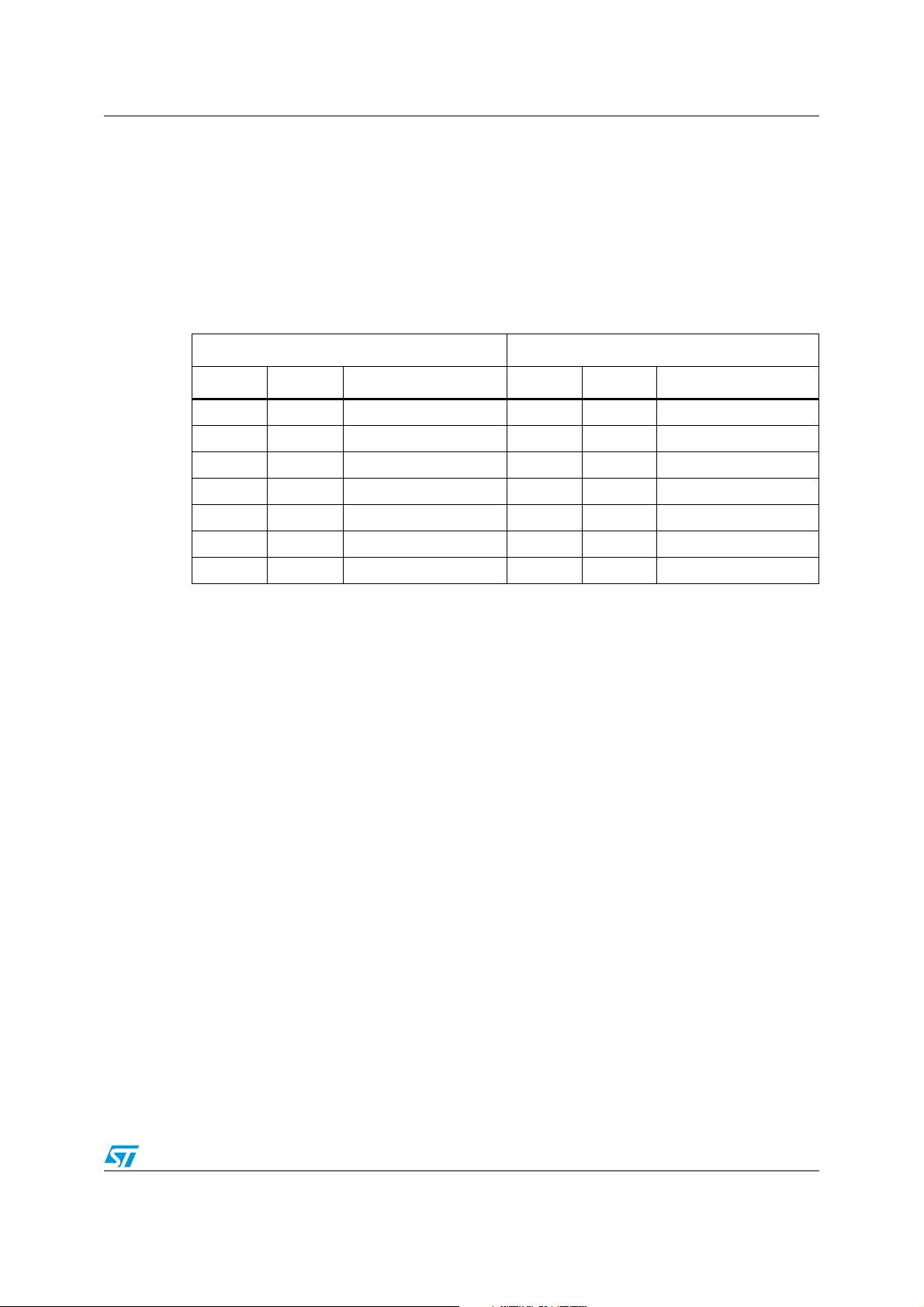
Table 1 lists the microcontrollers and development tools concerned by this application note.
Table 1. Applicable products
Type Product sub-class
Microcontroller
STM32 F0 Entry-level
STM32 F1 Mainstream
www.st.com
Contents AN4088
2/60 Doc ID 023072 Rev 1
Contents
1 Hardware migration . . . . . . . . . . . . . . . . . . . . . . . . . . . . . . . . . . . . . . . . . . 5
2 Boot mode compatibility . . . . . . . . . . . . . . . . . . . . . . . . . . . . . . . . . . . . . 6
3 Peripheral migration . . . . . . . . . . . . . . . . . . . . . . . . . . . . . . . . . . . . . . . . . 7
3.1 STM32 product cross-compatibility . . . . . . . . . . . . . . . . . . . . . . . . . . . . . . 7
3.2 System architecture . . . . . . . . . . . . . . . . . . . . . . . . . . . . . . . . . . . . . . . . . . 9
3.3 Memory mapping . . . . . . . . . . . . . . . . . . . . . . . . . . . . . . . . . . . . . . . . . . . 10
3.4 Reset and clock controller (RCC) interface . . . . . . . . . . . . . . . . . . . . . . . 13
3.5 DMA interface . . . . . . . . . . . . . . . . . . . . . . . . . . . . . . . . . . . . . . . . . . . . . . 16
3.6 Interrupt vectors . . . . . . . . . . . . . . . . . . . . . . . . . . . . . . . . . . . . . . . . . . . . 19
3.7 GPIO interface . . . . . . . . . . . . . . . . . . . . . . . . . . . . . . . . . . . . . . . . . . . . . 21
3.8 EXTI source selection . . . . . . . . . . . . . . . . . . . . . . . . . . . . . . . . . . . . . . . 23
3.9 FLASH interface . . . . . . . . . . . . . . . . . . . . . . . . . . . . . . . . . . . . . . . . . . . . 23
3.10 ADC interface . . . . . . . . . . . . . . . . . . . . . . . . . . . . . . . . . . . . . . . . . . . . . . 24
3.11 PWR interface . . . . . . . . . . . . . . . . . . . . . . . . . . . . . . . . . . . . . . . . . . . . . 26
3.12 Real-time clock (RTC) interface . . . . . . . . . . . . . . . . . . . . . . . . . . . . . . . . 27
3.13 SPI interface . . . . . . . . . . . . . . . . . . . . . . . . . . . . . . . . . . . . . . . . . . . . . . . 27
3.14 I2C interface . . . . . . . . . . . . . . . . . . . . . . . . . . . . . . . . . . . . . . . . . . . . . . . 28
3.15 USART interface . . . . . . . . . . . . . . . . . . . . . . . . . . . . . . . . . . . . . . . . . . . . 29
3.16 CEC interface . . . . . . . . . . . . . . . . . . . . . . . . . . . . . . . . . . . . . . . . . . . . . . 30
4 Firmware migration using the library . . . . . . . . . . . . . . . . . . . . . . . . . . 31
4.1 Migration steps . . . . . . . . . . . . . . . . . . . . . . . . . . . . . . . . . . . . . . . . . . . . . 31
4.2 RCC driver . . . . . . . . . . . . . . . . . . . . . . . . . . . . . . . . . . . . . . . . . . . . . . . . 31
4.3 FLASH driver . . . . . . . . . . . . . . . . . . . . . . . . . . . . . . . . . . . . . . . . . . . . . . 33
4.4 CRC driver . . . . . . . . . . . . . . . . . . . . . . . . . . . . . . . . . . . . . . . . . . . . . . . . 35
4.5 GPIO configuration update . . . . . . . . . . . . . . . . . . . . . . . . . . . . . . . . . . . . 36
4.5.1 Output mode . . . . . . . . . . . . . . . . . . . . . . . . . . . . . . . . . . . . . . . . . . . . . 36
4.5.2 Input mode . . . . . . . . . . . . . . . . . . . . . . . . . . . . . . . . . . . . . . . . . . . . . . . 36
4.5.3 Analog mode . . . . . . . . . . . . . . . . . . . . . . . . . . . . . . . . . . . . . . . . . . . . . 37
4.5.4 Alternate function mode . . . . . . . . . . . . . . . . . . . . . . . . . . . . . . . . . . . . . 37
AN4088 Contents
Doc ID 023072 Rev 1 3/60
4.6 EXTI Line0 . . . . . . . . . . . . . . . . . . . . . . . . . . . . . . . . . . . . . . . . . . . . . . . . 38
4.7 NVIC interrupt configuration . . . . . . . . . . . . . . . . . . . . . . . . . . . . . . . . . . . 39
4.8 ADC configuration . . . . . . . . . . . . . . . . . . . . . . . . . . . . . . . . . . . . . . . . . . 40
4.9 DAC driver . . . . . . . . . . . . . . . . . . . . . . . . . . . . . . . . . . . . . . . . . . . . . . . . 42
4.10 PWR driver . . . . . . . . . . . . . . . . . . . . . . . . . . . . . . . . . . . . . . . . . . . . . . . . 43
4.11 Backup data registers . . . . . . . . . . . . . . . . . . . . . . . . . . . . . . . . . . . . . . . . 44
4.12 CEC application code . . . . . . . . . . . . . . . . . . . . . . . . . . . . . . . . . . . . . . . . 45
4.13 I2C driver . . . . . . . . . . . . . . . . . . . . . . . . . . . . . . . . . . . . . . . . . . . . . . . . . 47
4.14 SPI driver . . . . . . . . . . . . . . . . . . . . . . . . . . . . . . . . . . . . . . . . . . . . . . . . . 51
4.15 USART driver . . . . . . . . . . . . . . . . . . . . . . . . . . . . . . . . . . . . . . . . . . . . . . 53
4.16 IWDG driver . . . . . . . . . . . . . . . . . . . . . . . . . . . . . . . . . . . . . . . . . . . . . . . 58
5 Revision history . . . . . . . . . . . . . . . . . . . . . . . . . . . . . . . . . . . . . . . . . . . 59
List of tables AN4088
4/60 Doc ID 023072 Rev 1
List of tables
Table 1. Applicable products . . . . . . . . . . . . . . . . . . . . . . . . . . . . . . . . . . . . . . . . . . . . . . . . . . . . . . . 1
Table 2. STM32F1 series and STM32F0 series pinout differences . . . . . . . . . . . . . . . . . . . . . . . . . . 5
Table 3. Boot modes. . . . . . . . . . . . . . . . . . . . . . . . . . . . . . . . . . . . . . . . . . . . . . . . . . . . . . . . . . . . . . 6
Table 4. STM32 peripheral compatibility analysis F1 versus F0 series . . . . . . . . . . . . . . . . . . . . . . . 8
Table 5. IP bus mapping differences between STM32F0 and STM32F1 series. . . . . . . . . . . . . . . . 10
Table 6. RCC differences between STM32F1 and STM32F0 series . . . . . . . . . . . . . . . . . . . . . . . . 13
Table 7. Example of migrating system clock configuration code from F1 to F0 . . . . . . . . . . . . . . . . 15
Table 8. RCC registers used for peripheral access configuration. . . . . . . . . . . . . . . . . . . . . . . . . . . 16
Table 9. DMA request differences between STM32F1 series and STM32F0 series . . . . . . . . . . . . 17
Table 10. Interrupt vector differences between STM32F1 series and STM32F0 series. . . . . . . . . . . 19
Table 11. GPIO differences between STM32F1 series and STM32F0 series . . . . . . . . . . . . . . . . . . 21
Table 12. FLASH differences between STM32F1 series and STM32F0 series . . . . . . . . . . . . . . . . . 23
Table 13. ADC differences between STM32F1 series and STM32F0 series . . . . . . . . . . . . . . . . . . . 24
Table 14. PWR differences between STM32F1 series and STM32F0 series. . . . . . . . . . . . . . . . . . . 26
Table 15. STM32F10x and STM32F0xx source clock API correspondence . . . . . . . . . . . . . . . . . . . 32
Table 16. STM32F10x and STM32F0xx FLASH driver API correspondence. . . . . . . . . . . . . . . . . . . 33
Table 17. STM32F10xx and STM32F0xx CRC driver API correspondence. . . . . . . . . . . . . . . . . . . . 35
Table 18. STM32F10x and STM32F0xx MISC driver API correspondence . . . . . . . . . . . . . . . . . . . . 40
Table 19. STM32F10x and STM32F0xx DAC driver API correspondence. . . . . . . . . . . . . . . . . . . . . 42
Table 20. STM32F10x and STM32F0xx PWR driver API correspondence . . . . . . . . . . . . . . . . . . . . 43
Table 21. STM32F10xx and STM32F0xx CEC driver API correspondence . . . . . . . . . . . . . . . . . . . . 45
Table 22. STM32F10xx and STM32F0xx I2C driver API correspondence . . . . . . . . . . . . . . . . . . . . . 47
Table 23. STM32F10xx and STM32F0xx SPI driver API correspondence. . . . . . . . . . . . . . . . . . . . . 51
Table 24. STM32F10x and STM32F0xx USART driver API correspondence . . . . . . . . . . . . . . . . . . 54
Table 25. STM32F10xx and STM32Fxx IWDG driver API correspondence. . . . . . . . . . . . . . . . . . . . 58
Table 26. Document revision history . . . . . . . . . . . . . . . . . . . . . . . . . . . . . . . . . . . . . . . . . . . . . . . . . 59
AN4088 Hardware migration
Doc ID 023072 Rev 1 5/60
1 Hardware migration
The entry-level STM32F0 and general-purpose STM32F1xxx families are pin-to-pin
compatible. All peripherals shares the same pins in the two families, but there are some
minor differences between packages. The transition from the STM32F1 series to the
STM32F0 series is simple as only a few pins are impacted (impacted pins are in bold in
Tabl e 2 ).
The migration from F1 to F0 has no impact on the pinout, except that the user wins 2 or 4
GPIOs for his/her application at VSS/VDD 2 and 4 locations, depending on the package
used.
Table 2. STM32F1 series and STM32F0 series pinout differences
STM32F1 series STM32F0 series
QFP48 QFP64 Pinout QFP48 QFP64 Pinout
55PD0 - OSC_IN 5 5 PH0 - OSC_IN
66PD1 - OSC_OUT 6 6 PH1 - OSC_OUT
-18VSS_4 -18PF4
-19VDD_4 -19PF5
35 47 VSS_2 35 47 PF6
36 48 VDD_2 36 48 PF7
20 28 Boot1/PB2 20 28 PB2
剩余59页未读,继续阅读
fengqiyeluo2012
- 粉丝: 0
- 资源: 1
上传资源 快速赚钱
- 我的内容管理 收起
- 我的资源 快来上传第一个资源
- 我的收益 登录查看自己的收益
- 我的积分 登录查看自己的积分
- 我的C币 登录后查看C币余额
- 我的收藏
- 我的下载
- 下载帮助
会员权益专享
最新资源
- 保险服务门店新年工作计划PPT.pptx
- 车辆安全工作计划PPT.pptx
- ipqc工作总结PPT.pptx
- 车间员工上半年工作总结PPT.pptx
- 保险公司员工的工作总结PPT.pptx
- 报价工作总结PPT.pptx
- 冲压车间实习工作总结PPT.pptx
- ktv周工作总结PPT.pptx
- 保育院总务工作计划PPT.pptx
- xx年度现代教育技术工作总结PPT.pptx
- 出纳的年终总结PPT.pptx
- 贝贝班班级工作计划PPT.pptx
- 变电值班员技术个人工作总结PPT.pptx
- 大学生读书活动策划书PPT.pptx
- 财务出纳月工作总结PPT.pptx
- 大学生“三支一扶”服务期满工作总结(2)PPT.pptx
资源上传下载、课程学习等过程中有任何疑问或建议,欢迎提出宝贵意见哦~我们会及时处理!
点击此处反馈
安全验证
文档复制为VIP权益,开通VIP直接复制
信息提交成功