2N3904三极管参数资料
2N3904三极管参数资料
2N3904三极管参数资料
2N3904三极管参数资料
Rev. A, February 2003
NPN General Purpose Amplifier
This device is designed as a general purpose amplifier and switch.
The useful dynamic range extends to 100mA as a switch and to
100 MHz as an amplifier.
Absolute Maximum Ratings* T
A
=25
o
C unless otherwise noted
Symbol Parameter Value Units
V
CEO
Collector-Emitter Voltage 40 V
V
CBO
Collector-Base Voltage 60 V
V
EBO
Emitter-Base Voltage 6.0 V
I
C
Collector Current – Continuous 200 mA
T
J
, T
STG
Operating and Storage Junction Temperature Range -55 to +150
o
C
*These ratings are limiting values above which the serviceability of any semiconductor device may be impaired.
NOTES:
1) These ratings are based on a maximum junction temperature of 150 degrees C.
2) These are steady state limits. The factory should be consulted on applications involving pulsed or low duty cycle operations.
Thermal Characteristics T
A
=25
o
C unless otherwise noted
Symbol Characteristic Max Units
2N3904 MMBT3904
P
D
Total Device Dissipation
Derate above 25
o
C
625
5.0
350
2.8
mW
mW/
o
C
R
èJC
Thermal Resistance, Junction to Case 83.3
o
C /W
R
èJA
Thermal Resistance, Junction to Ambient 200 375
o
C /W
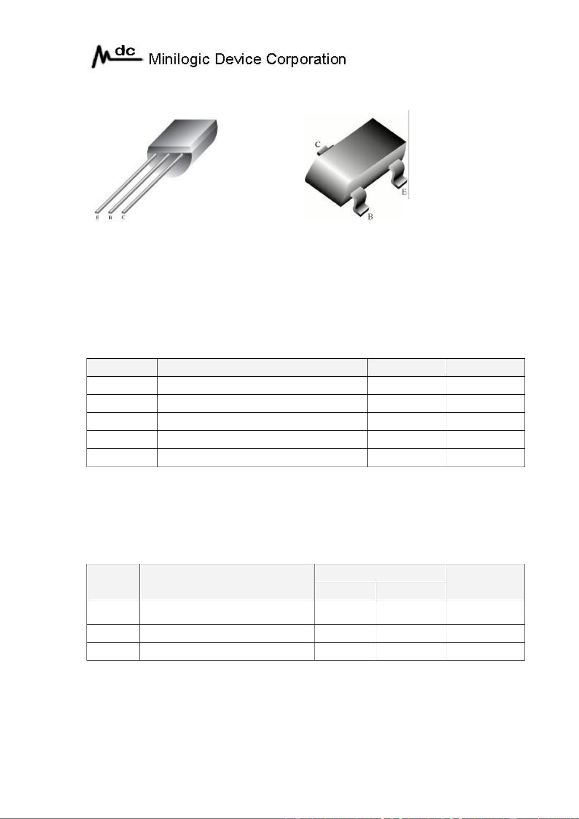
2N3904
TO-92
E:Emitter B:Base C:Collector
MMBT3904
SOT-23
下载后可阅读完整内容,剩余0页未读,立即下载
2024-05-01 上传
2024-02-06 上传
2023-12-31 上传
2024-08-28 上传
2024-10-23 上传
2023-05-11 上传

yanguopu
- 粉丝: 0
- 资源: 14
 我的内容管理
展开
我的内容管理
展开


最新资源
- Raspberry Pi OpenCL驱动程序安装与QEMU仿真指南
- Apache RocketMQ Go客户端:全面支持与消息处理功能
- WStage平台:无线传感器网络阶段数据交互技术
- 基于Java SpringBoot和微信小程序的ssm智能仓储系统开发
- CorrectMe项目:自动更正与建议API的开发与应用
- IdeaBiz请求处理程序JAVA:自动化API调用与令牌管理
- 墨西哥面包店研讨会:介绍关键业绩指标(KPI)与评估标准
- 2014年Android音乐播放器源码学习分享
- CleverRecyclerView扩展库:滑动效果与特性增强
- 利用Python和SURF特征识别斑点猫图像
- Wurpr开源PHP MySQL包装器:安全易用且高效
- Scratch少儿编程:Kanon妹系闹钟音效素材包
- 食品分享社交应用的开发教程与功能介绍
- Cookies by lfj.io: 浏览数据智能管理与同步工具
- 掌握SSH框架与SpringMVC Hibernate集成教程
- C语言实现FFT算法及互相关性能优化指南
