TI ADS7028:8通道SPI ADC与GPIO功能详解
需积分: 5 193 浏览量
更新于2024-06-28
4
收藏 1.14MB PDF 举报
TI-ADS7028是一款小型8通道12位模数转换器(ADC),其设计紧凑,采用了WQFN3mm×3mm封装,适合于空间受限的应用。该设备具有高度灵活性,能够根据需要配置为8个模拟输入、数字输入或数字输出通道。其中,GPIO功能特别强大,支持漏极开路和推挽输出,以扩展I/O能力。
ADC的核心特性包括:
1. **模拟与数字输入/输出选择**:
- 用户可以根据项目需求选择模拟信号输入或者利用GPIO作为数字信号的输入/输出接口。
2. **GPIO功能**:
- GPIO提供了丰富的功能,如GPOWrite允许控制GPIO输出,而GPIRead则能读取GPIO的状态。此外,GPIO还支持数字信号的扩展和配置。
3. **可编程阈值与事件检测**:
- 每个通道都配备有可编程阈值,可以用于设置高/低电平触发点,同时还有用于瞬态抑制的事件计数器。
4. **宽工作电压和温度范围**:
- ADC支持两种工作电压:AVDD(2.35V 至 5.5V)和 DVDD(1.65V 至 5.5V),适应于较为广泛的电源环境。它还具备良好的温度耐受性,工作在-40°C至+85°C的极端条件下。
5. **增强型SPI接口**:
- ADS7028配备了高速的60MHz SPI接口,方便与其他微控制器或其他数字设备进行通信,且能实现高效的数据传输。
6. **数据校验功能**:
- 包含CRC(循环冗余校验)功能,确保数据通信的准确性。
7. **保护机制**:
- 提供了过电压保护(OVP)和过电流保护(OCP),以确保电路的安全运行。
该文档提供的中文版本信息主要是为了帮助用户理解和应用TI的产品,但建议在实际设计时,务必查阅最新的英文数据手册(SBAS978)以获取最准确的技术细节和规格。若需要技术支持、软件工具或社区交流,可通过TI官方网站获取完整且官方的支持资源。

ADVANCEINFORMATION
13
ADS7028
www.ti.com.cn
ZHCSJX5 –JUNE 2019
版权 © 2019, Texas Instruments Incorporated
When the ADS7028 detects a CRC error on the SPI interface, the erroneous data are ignored and the
CRCERR_IN bit is set. Additional notifications can be enabled as described in 表 2. Further register writes are
disabled until the CRCERR_IN bit is cleared by writing 1b to this bit. When using autonomous conversion mode,
further conversions can be disabled on a CRC error on the SPI interface by setting CONV_ON_ERR = 1b.
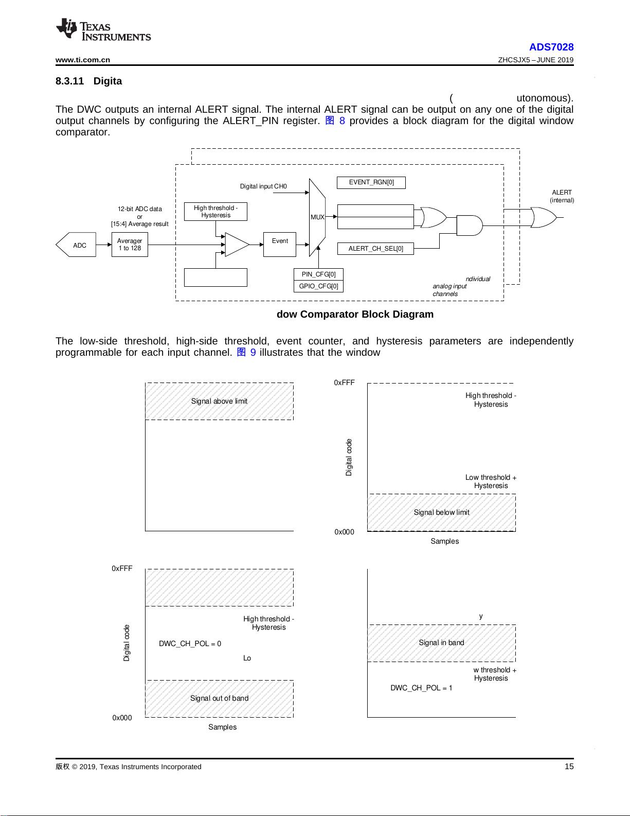
8.3.7 General-Purpose I/Os
The eight channels of the ADS7028 can be independently configured as analog inputs, digital inputs, or digital
outputs. 表 3 shows how the PIN_CFG and GPIO_CFG registers can be used to configure the device channels.
表表 3. Configuring Channels as Analog Inputs or GPIOs
PIN_CFG[7:0] GPIO_CFG[7:0] GPO_DRIVE_CFG[7:0] CHANNEL CONFIGURATION
0 x x Analog input (default)
1 0 x Digital input
1 1 0 Digital output; open-drain driver
1 1 1 Digital output; push-pull driver
Digital outputs can be configured to logic 1 or 0 by writing to the GPO_OUTPUT_VALUE register. Reading the
GPI_VALUE register returns the logic level for all channels configured as digital inputs or digital outputs. The
GPI_VALUE register can be read to detect a failure in external components, such as a floating pullup resistor or
a low-impedance pulldown resistor, that prevents digital outputs being set to the desired logic level.
8.3.8 Oscillator and Timing Control
The device uses an internal oscillator for conversion. When using the averaging module, the host initiates the
first conversion and subsequent conversions are generated internally by the device. Also, in autonomous mode
of operation, the start of the conversion signal is generated by the device. 表 4 describes how the sampling rate
can be controlled by the OSC_SEL and CLK_DIV[3:0] register fields when the device generates the start of the
conversion.
表表 4. Configuring Sampling Rate for Internal Conversion Start Control
CLK_DIV[3:0]
OSC_SEL = 0 OSC_SEL = 1
SAMPLING FREQUENCY, f
CYCLE
(kSPS)
CYCLE TIME,
t
CYCLE
(µs)
SAMPLING FREQUENCY,
f
CYCLE
(kSPS)
CYCLE TIME, t
CYCLE
(µs)
0000b 1000 1 31.25 32
0001b 666.7 1.5 20.83 48
0010b 500 2 15.63 64
0011b 333.3 3 10.42 96
0100b 250 4 7.81 128
0101b 166.7 6 5.21 192
0110b 125 8 3.91 256
0111b 83 12 2.60 384
1000b 62.5 16 1.95 512
1001b 41.7 24 1.3 768
1010b 31.3 32 0.98 1024
1011b 20.8 48 0.65 1536
1100b 15.6 64 0.49 2048
1101b 10.4 96 0.33 3072
The conversion time of the device, given by t
CONV
in the Switching Characteristics table, is independent of the
OSC_SEL and CLK_DIV[3:0] configuration.
8.3.9 Output Data Format
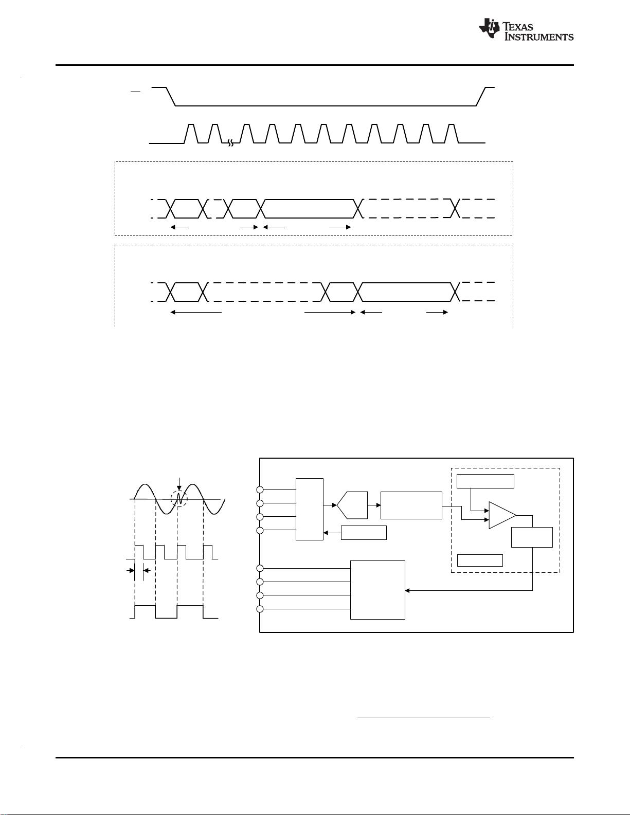
图 6 shows various SPI frames for reading data. The data output is MSB aligned. If averaging is enabled the
output data from the ADC are 16 bits long, otherwise the output data are 12 bits long. Optionally, a 4-bit channel
ID or status flags can be appended at the end of the output data by configuring the APPEND_STATUS[1:0] field.
剩余78页未读,继续阅读
点击了解资源详情
点击了解资源详情
点击了解资源详情
2022-11-27 上传
2022-11-27 上传
2022-11-27 上传
2022-12-04 上传
2022-12-04 上传
2022-11-27 上传

不觉明了
- 粉丝: 7394
- 资源: 5764
 我的内容管理
展开
我的内容管理
展开


最新资源
- srvany&instsrv.zip
- iss-lab
- project-decoder-ring:面向思考课程的Decoder Ring项目
- pathforajs:Web个性化SDK
- student manager.zip
- 2500字风险投资项目评估问题研究 (定稿)(3).zip
- SQL
- spring-websocket-test
- phytonecrosis-dev:植物版本
- CSM300V1.2.zip
- worklet-loader:用于工作包的Webpack加载器
- 2500字风险投资项目评估问题研究 (定稿)(1).zip
- Birdwatching:Mountain Birdwatch 1.0监视程序分析和可视化
- Jhonathan_Seo
- ASRFrame:An Automatic Speech Recognition Frame ,一个中文语音识别的完整框架, 提供了多个模型
- AmaterasUML_1.3.4 (1).zip
