CS8413 CS8414
DS240F1 7
GENERAL DESCRIPTION
The CS8413/14 are monolithic CMOS circuits that
receive and decode audio and digital data accord-
ing to the AES/EBU, IEC 958, S/PDIF, and EIAJ
CP340/1201 interface standards. Both chips con-
tain RS422 line receivers and Phase-Locked Loops
(PLL) that recover the clock and synchronization
signals, and de-multiplex the audio and digital data.
The CS8413 contains a configurable internal buffer
memory, read via a parallel port, which can buffer
channel status, user, and optionally auxiliary data.
The CS8414 de-multiplexes the channel status, us-
er, and validity information directly to serial output
pins with dedicated pins for the most important
channel status bits. Both chips also contain exten-
sive error reporting as well as incoming sample fre-
quency indication for auto-set applications.
The CS8413/14 are pin-compatible with the
CS8411/12 digital audio receiver parts. The func-
tionality of the CS8413/14 is the same as the
CS8411/12 with two exceptions: first, the operat-
ing frequency (sample rate) of the CS8413/14 is ex-
tended to include 96 kHz, and second, the
frequency reporting bits are modified to delete the
±400 ppm ranges, and include 88.2 kHz and
96 kHz ranges.
Familiarity with the AES/EBU and IEC 958 speci-
fications are assumed throughout this document.
The App Note, Overview of Digital Audio Inter-
face Data Structures, contains information on digi-
tal audio specifications; however, it is not meant to
be a complete reference. To guarantee compliance,
the proper standards documents should be ob-
tained. The AES/EBU standard, AES3-1985,
should be obtained from the Audio Engineering
Society or ANSI (ANSI document # ANSI S4.40-
1985); the IEC 958 standard from the International
Electrotechnical Commission; and the EIAJ
CP340/1201 standard from the Japanese Electron-
ics Bureau.
Line Receiver
The RS422 line receiver can decode differential as
well as single ended inputs. The receiver consists
of a differential input Schmitt trigger with 50mV of
hysteresis. The hysteresis prevents noisy signals
from corrupting the phase detector. Appendix A
contains more information on how to configure the
line receivers for differential and single ended sig-
nals.
Clocks and Jitter Attenuation
The primary function of these chips is to recover
audio data and low jitter clocks from a digital audio
transmission line. The clocks that can be generated
are MCK (256xF
S
), SCK (64xF
S
), and FSYNC (F
S
or 2xF
S
). MCK is the output of the voltage con-
trolled oscillator which is a component of the PLL.
The PLL consists of phase and frequency detectors,
a second-order loop filter, and a voltage controlled
oscillator. All components of the PLL are on chip
with the exception of a resistor and capacitor used
in the loop filter. This filter is connected between
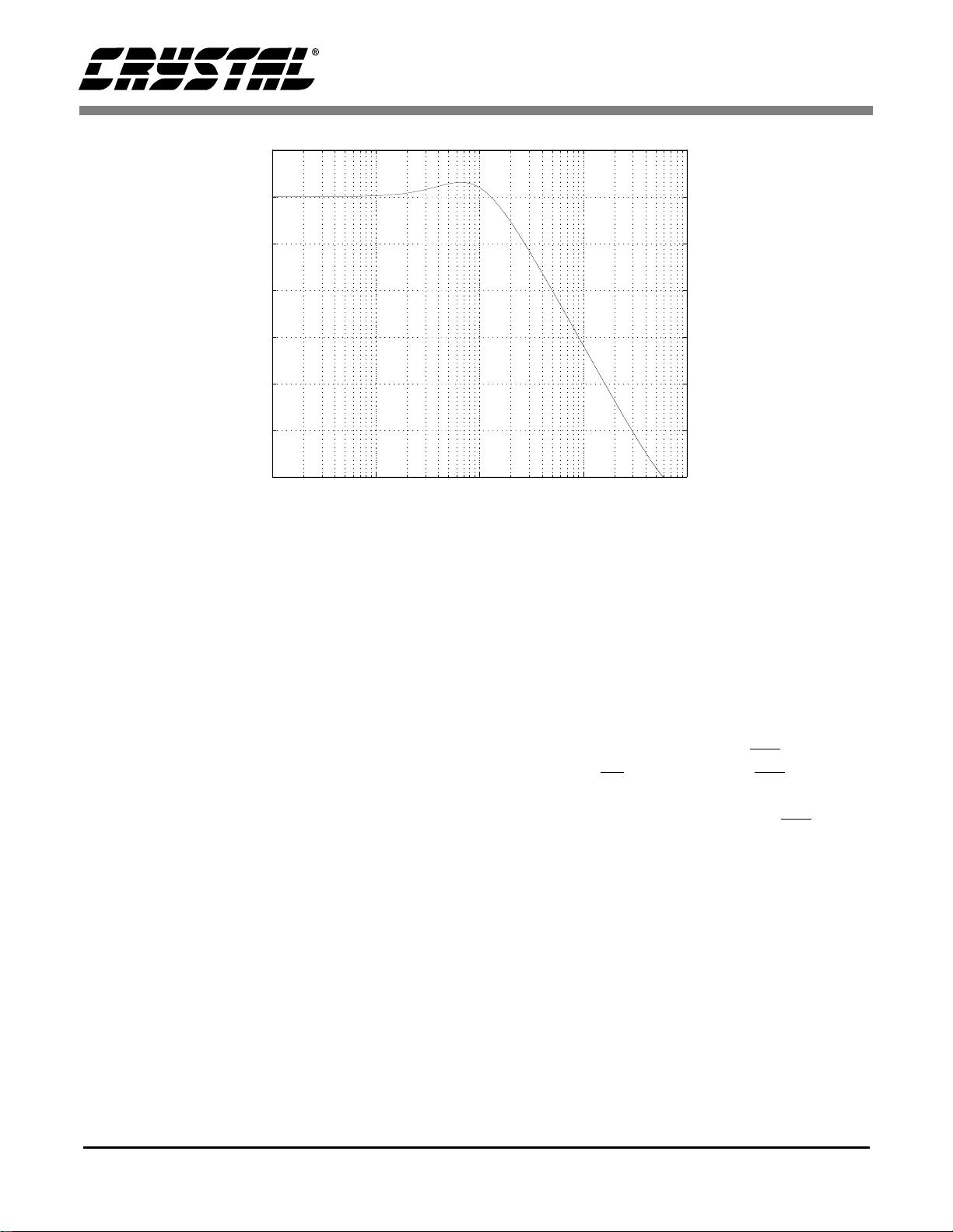
the FILT pin and AGND. The typical closed-loop
transfer function, which specifies the PLL’s jitter
attenuation characteristics, is shown in Figure 3.
Most jitter introduced by the transmission line is
high in frequency and will be strongly attenuated.
Multiple frequency detectors are used to minimize
the time it takes the PLL to lock to the incoming
data stream and to prevent false lock conditions.
When the PLL is not locked to the incoming data
stream, the frequency detectors pull the VCO fre-
quency within the lock range of the PLL. When no
digital audio data is present, the VCO frequency is
pulled to its minimum value.
As a master, SCK is always MCK divided by four,
producing a frequency of 64xF
S
. In the CS8413,
FSYNC can be programmed to be a divided version
of MCK or it can be generated directly from the in-
coming data stream. In the CS8414, FSYNC is al-
ways generated from the incoming data stream.
When FSYNC is generated from the data, its edges


