


MAX3485系列:低功耗RS-485/RS-422通信收发器详解
需积分: 48 6 浏览量
更新于2024-07-14
收藏 199KB PDF 举报
MAX3485数据手册详细介绍了该系列的低功耗RS-485和RS-422通信收发器,包括MAX3483、MAX3485、MAX3486、MAX3488、MAX3490和MAX3491。这些器件的特点显著,设计用于在各种通信应用中提供高效、低噪声的数据传输。
首先,MAX3483和MAX3488特别注重驱动器的特性,它们配备了限流驱动器,通过抑制电磁干扰(EMI)和减少由于电缆不恰当终端引起的反射,确保在高达250kbps的数据速率下实现无错误的数据传输。这部分的限流设计有助于保护设备免受电源波动的影响,并提供更稳定的通信环境。
MAX3486则采用部分限流驱动器技术,可以达到更高的数据传输速度,可达2.5Mbps,适合对速度有更高要求的应用场景。而MAX3485、MAX3490和MAX3491支持更高速度,可达到10Mbps,适用于需要快速数据交换的场合。
所有这些器件都具有短路电流限制功能,能保护驱动器免受过载损坏,并通过热关断电路防止过度功率消耗,确保了系统的可靠性和稳定性。此外,接收器输入设计有安全机制,当两个输入都处于开路状态时,保证输出逻辑高电平,增加了系统的鲁棒性。
MAX3488、MAX3490和MAX3491具备全双工通信能力,允许数据在发送和接收同时进行,而MAX3483、MAX3485和MAX3486则专为半双工通信设计,适用于单向或双向但非同时的数据流。
这些收发器广泛应用于低功耗RS-485/RS-422通信系统中,特别是在电信通信领域,它们能够为工业自动化、物联网(IoT)设备、远程监控和智能电网等应用提供稳定、高效的通信解决方案。同时,由于其抗干扰能力和高可靠性,它们也是构建EMI敏感设备的理想选择。MAX3485系列是实现长距离、低能耗通信的理想选择,适用于需要在各种环境下维持高质量数据传输的场合。
MAX3483/MAX3485/MAX3486/MAX3488/MAX3490/MAX3491
3.3V-Powered, 10Mbps and Slew-Rate-Limited
True RS-485/RS-422 Transceivers
4 _______________________________________________________________________________________
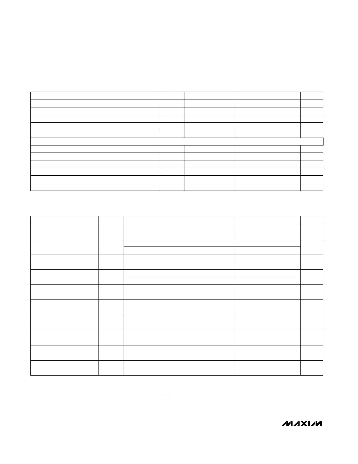
DRIVER SWITCHING CHARACTERISTICS—MAX3483 and MAX3488
(V
CC
= 3.3V, T
A
= +25°C)
ns50 80t
PLZ
Driver Output Disable Time from Low Level R
L
= 110Ω, Figure 10
ns700 1000 1500t
PLH
Driver Propagation Delay, Low-to-High Level
ns400 700 1200t
TD
ns600 900 1400t
DD
Driver Differential Output Delay
Driver Differential Output Transition Time
µs2.2 3.0t
PSH
Driver Output Enable Time from Shutdown to High Level
µs1.9 2.7t
PSL
Driver Output Enable Time from Shutdown to Low Level
ns50 80t
PHZ
Driver Output Disable Time from High Level
ns700 1000 1500t
PHL
Driver Propagation Delay, High-to-Low Level
ns100t
PDS
|
t
PLH
- t
PHL|
Driver Propagation Delay Skew (Note 2)
ns900 1300t
PZL
Driver Output Enable Time to Low Level
ns600 800t
PZH
Driver Output Enable Time to High Level
UNITSMIN TYP MAXSYMBOLPARAMETER
R
L
= 27Ω, Figure 8
R
L
= 60Ω, Figure 7
R
L
= 60Ω, Figure 7
R
L
= 110Ω, Figure 9
R
L
= 110Ω, Figure 10
R
L
= 110Ω, Figure 9
R
L
= 27Ω, Figure 8
R
L
= 27Ω, Figure 8
R
L
= 110Ω, Figure 10
R
L
= 110Ω, Figure 9
CONDITIONS
RECEIVER SWITCHING CHARACTERISTICS
(V
CC
= 3.3V, T
A
= +25°C)
ns25 45t
PRLZ
Receiver Output Disable
Time from Low Level
C
L
= 15pF, Figure 12,
MAX3483/MAX3485/MAX3486/MAX3491 only
ns
25 65 90
ns80 190 300t
SHDN
Time to Shutdown
ns720 1400t
PRSH
Receiver Output Enable Time
from Shutdown to High Level
ns720 1400t
PRSL
Receiver Output Enable Time
from Shutdown to Low Level
ns25 45t
PRHZ
Receiver Output Disable
Time from High Level
ns
25 65 90
ns
10
ns25 50t
PRZL
Receiver Output Enable Time
to Low Level
ns25 50t
PRZH
Receiver Output Enable Time
to High Level
UNITSMIN TYP MAXSYMBOLPARAMETER
V
ID
= 0V to 3.0V, C
L
= 15pF, Figure 11
MAX3483/MAX3485/MAX3486/MAX3491 only
(Note 3)
C
L
= 15pF, Figure 12,
MAX3483/MAX3485/MAX3486/MAX3491 only
C
L
= 15pF, Figure 12,
MAX3483/MAX3485/MAX3486/MAX3491 only
C
L
= 15pF, Figure 12,
MAX3483/MAX3485/MAX3486/MAX3491 only
V
ID
= 0V to 3.0V, C
L
= 15pF, Figure 11
V
ID
= 0V to 3.0V, C
L
= 15pF, Figure 11
C
L
= 15pF, Figure 12,
MAX3483/MAX3485/MAX3486/MAX3491 only
C
L
= 15pF, Figure 12,
MAX3483/MAX3485/MAX3486/MAX3491 only
CONDITIONS
25 75 120
t
RPLH
Receiver Propagation Delay,
Low-to-High Level
MAX3483/MAX3488
25 75 120
t
RPHL
Receiver Propagation Delay,
High-to-Low Level
MAX3483/MAX3488
20
t
RPDS
|
t
PLH
- t
PHL|
Receiver
Propagation Delay Skew
MAX3483/MAX3488
Note 1: ∆V
OD
and ∆V
OC
are the changes in V
OD
and V
OC
, respectively, when the DI input changes state.
Note 2: Measured on
|
t
PLH
(Y) - t
PHL
(Y)
|
and
|
t
PLH
(Z) - t
PHL
(Z)
|.
Note 3: The transceivers are put into shutdown by bringing RE high and DE low. If the inputs are in this state for less than 80ns, the
parts are guaranteed not to enter shutdown. If the inputs are in this state for at least 300ns, the parts are guaranteed to
have entered shutdown. See
Low-Power Shutdown Mode
section.
DRIVER OUTPUT ENABLE/DISABLE TIMES (MAX3483 only)
下载后可阅读完整内容,剩余15页未读,立即下载
2221 浏览量
2011-03-28 上传
140 浏览量
216 浏览量
2020-04-17 上传
260 浏览量

qq_34346151
- 粉丝: 0
 我的内容管理
展开
我的内容管理
展开


最新资源
- Findbugs插件在MyEclipse 10中的集成指南
- Android实现吹一吹功能的详细教程
- 开放arm-mp3源代码资源,鼓励技术交流学习
- IEEE 802.3标准2000年版介绍
- Win32 API入门:Socket网络编程示例
- 深入探讨Spring框架中的公共属性注入技术
- 深入解析TCP/IP协议:C语言源代码剖析
- JSP文件上传功能实现教程与源码分析
- Python库eefbrain版本0.29.5发布,支持MacOS
- Struts框架实现登录功能教程与示例
- 掌握GridBagConstraints:JAVA布局模式技巧全解析
- 图像处理技术的应用与实践
- 74LS系列芯片全面解析:功能特点与应用简介
- 打造类VisualStudio列表框控件类
- 实现智能搜索提示的jQuery搜索栏教程
- 探索vi/vim编辑器的键盘快捷键图