DR
AFT
DR
AFT
DRAFT
DR
D
RAFT
DRAFT
DRA
F
T DRAF
D
RAFT DRAFT DRAFT DRAFT DRAFT D
DRAFT
D
RAFT DRA
F
T DRAFT DRAFT DRAFT DRA
UM10360_0 © NXP B.V. 2009. All rights reserved.
User manual Rev. 00.06 — 5 June 2009 19 of 808
NXP Semiconductors
UM10360
Chapter 3: LPC17xx System control
4.1 Reset Source Identification Register (RSID - 0x400F C180)
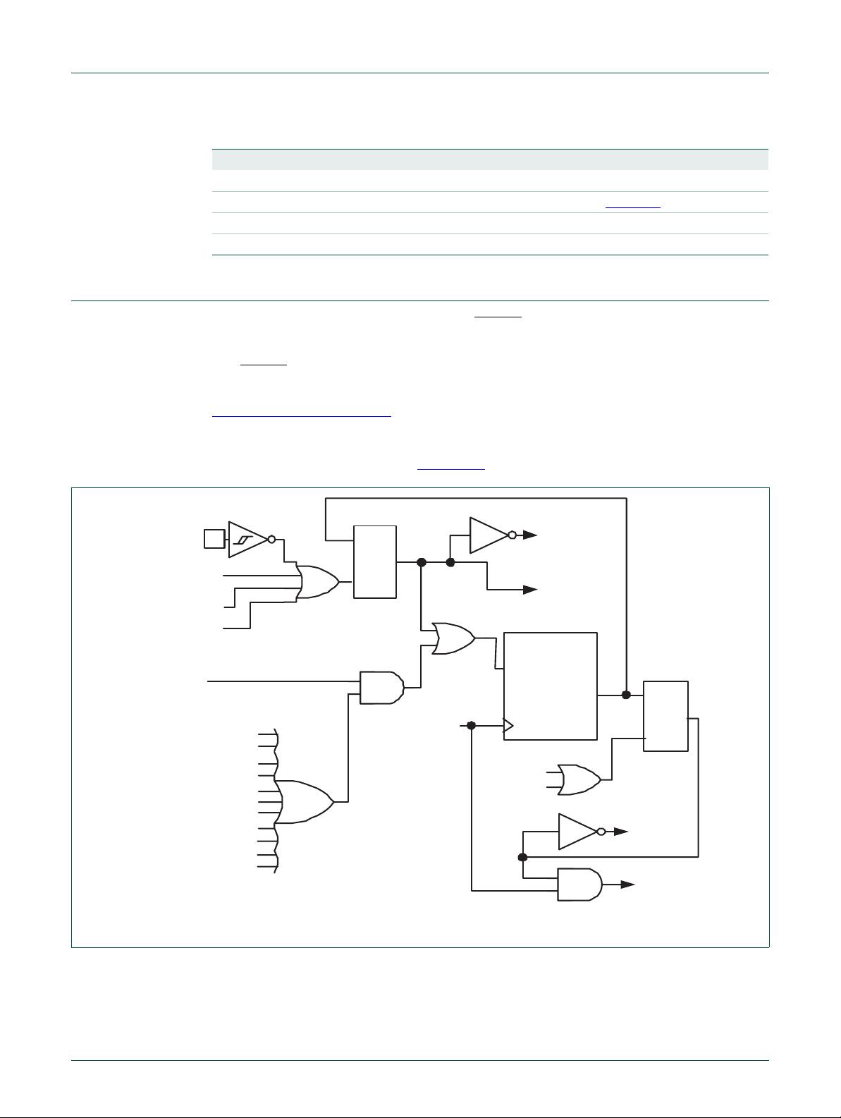
This register contains one bit for each source of Reset. Writing a 1 to any of these bits
clears the corresponding read-side bit to 0. The interactions among the four sources are
described below.
5. Brown-out detection
The LPC17xx includes 2-stage monitoring of the voltage on the V
DD(REG)(3V3)
pins. If this
voltage falls below 2.9 V, the Brown-Out Detector (BOD) asserts an interrupt signal to the
Vectored Interrupt Controller. This signal can be enabled for interrupt in the Interrupt
Enable Register in the NVIC in order to cause a CPU interrupt; if not, software can monitor
the signal by reading the Raw Interrupt Status Register.
The second stage of low-voltage detection asserts Reset to inactivate the LPC17xx when
the voltage on the V
DD(REG)(3V3)
pins falls below 2.6 V. This Reset prevents alteration of
the flash as operation of the various elements of the chip would otherwise become
unreliable due to low voltage. The BOD circuit maintains this reset down below 1 V, at
which point the Power-On Reset circuitry maintains the overall Reset.
Both the 2.9 V and 2.6 V thresholds include some hysteresis. In normal operation, this
hysteresis allows the 2.9 V detection to reliably interrupt, or a regularly-executed event
loop to sense the condition.
Table 8. Reset Source Identification register (RSID - address 0x400F C180) bit description
Bit Symbol Description Reset
value
0 POR Assertion of the POR signal sets this bit, and clears all of the other bits in
this register. But if another Reset signal (e.g., External Reset) remains
asserted after the POR signal is negated, then its bit is set. This bit is not
affected by any of the other sources of Reset.
See text
1 EXTR Assertion of the RESET
signal sets this bit. This bit is cleared by POR,
but is not affected by WDT or BOD reset.
See text
2 WDTR This bit is set when the Watchdog Timer times out and the WDTRESET
bit in the Watchdog Mode Register is 1. It is cleared by any of the other
sources of Reset.
See text
3 BODR This bit is set when the V
DD(REG)(3V3)
voltage reaches a level below
2.6 V.
If the V
DD(REG)(3V3)
voltage dips from 3.3 V to 2.5 V and recovers, the
BODR bit will be set to 1.
If the V
DD(REG)(3V3)
voltage dips from 3.3 V to 2.5 V and continues to
decline to the level at which POR is asserted (nominally 1 V), the BODR
bit is cleared.
If the V
DD(REG)(3V3)
voltage rises continuously from below 1 V to a level
above 2.6 V, the BODR will be set to 1.
This bit is not affected by External Reset nor Watchdog Reset.
Note: Only in the case where a reset occurs and the POR = 0, the
BODR bit indicates if the V
DD(REG)(3V3)
voltage was below 2.6 V or not.
See text
7:4 - Reserved, user software should not write ones to reserved bits. The
value read from a reserved bit is not defined.
NA


