XR16C854 UART扩展技术详解:4通道串口与128字节FIFO
需积分: 15 161 浏览量
更新于2024-07-16
收藏 752KB PDF 举报
XR16C854/854D是一款由Exar Corporation生产的高性能串口扩展芯片,其版本为Rev.3.1.0,发布于2013年4月。这款芯片的主要特点是集成了四个独立的通用异步接收器和发射器(UART),每个 UART 都配备有128字节的传输和接收 FIFO(先进先出队列),支持硬件和软件流控制,数据传输速率最高可达2Mbps。
该芯片提供了丰富的功能,用户可以通过一组寄存器进行操作状态监控、控制以及错误指示。它具有灵活的系统中断设计,允许根据设计需求定制中断处理,便于进行故障诊断。内部的环回功能使得芯片在板上就能进行自我诊断测试。
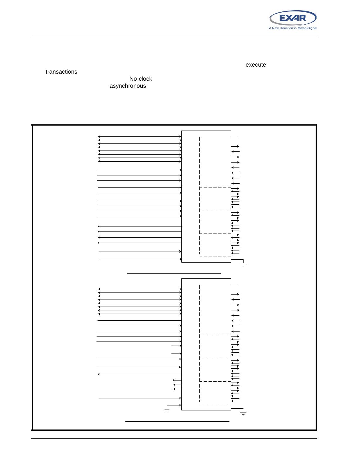
XR16C854/854D支持两种模式接口:16模式接口和额外的68模式接口。其中,64引脚LQFP封装仅提供16模式接口,而68引脚PLCC和100引脚QFP封装则额外支持68模式接口,这对于与摩托罗拉处理器的无缝集成特别有用,简化了设计流程。
值得一提的是,XR16C854CV型号提供了三个状态中断输出选项,适合对中断信号类型有不同需求的应用;而XR16C854DV则提供连续中断输出,这意味着它能够连续产生中断请求,提高了系统的响应速度和实时性。
XR16C854/854D是一款适用于多种通信场景的高效串口扩展解决方案,特别适合需要高带宽、低延迟和灵活中断管理的工业控制、物联网设备以及嵌入式系统设计。为了更深入地了解和利用这款芯片,建议参考文档中的详细规格、功能描述以及示例电路设计,以便根据具体项目需求进行优化配置和应用。
XR16C854/854D
9
REV. 3.1.0
2.97V TO 5.5V QUAD UART WITH 128-BYTE FIFO
1.0 PRODUCT DESCRIPTION
The XR16C854 (854) integrates the functions of 4 enhanced 16C550 Universal Asynchronous Receiver and
Transmitter (UART). Each UART is independently controlled having its own set of device configuration
registers. The configuration registers set is 16550 UART compatible for control, status and data transfer.
Additionally, each UART channel has 128-bytes of transmit and receive FIFOs, automatic RTS/CTS hardware
flow control with hysteresis control, automatic Xon/Xoff and special character software flow control,
programmable transmit and receive FIFO trigger levels, FIFO level counters, infrared encoder and decoder
(IrDA ver 1.0), programmable baud rate generator with a prescaler of divide by 1 or 4, and data rate up to 2
Mbps. The XR16C854 can operate at 3.3 or 5 volts. The 854 is fabricated with an advanced CMOS process.
Enhanced FIFO
The 854 QUART provides a solution that supports 128 bytes of transmit and receive FIFO memory, instead of
64 bytes provided in the ST16C654 and 16 bytes in the ST16C554, or one byte in the ST16C454. The 854 is
designed to work with high performance data communication systems, that require fast data processing time.
Increased performance is realized in the 854 by the larger transmit and receive FIFOs, FIFO trigger level
control, FIFO level counters and automatic flow control mechanism. This allows the external processor to
handle more networking tasks within a given time. For example, the ST16C554 with a 16 byte FIFO, unloads
16 bytes of receive data in 1.53 ms (This example uses a character length of 11 bits, including start/stop bits at
115.2Kbps). This means the external CPU will have to service the receive FIFO at 1.53 ms intervals. However
with the 128 byte FIFO in the 854, the data buffer will not require unloading/loading for 12.2 ms. This increases
the service interval giving the external CPU additional time for other applications and reducing the overall
UART interrupt servicing time. In addition, the programmable FIFO level trigger interrupt and automatic
hardware/software flow control is uniquely provided for maximum data throughput performance especially
when operating in a multi-channel system. The combination of the above greatly reduces the CPU’s bandwidth
requirement, increases performance, and reduces power consumption.
Data Rate
The 854 is capable of operation up to 2 Mbps at 5V with 16x internal sampling clock rate. The device can
operate with a crystal oscillator of up to 24 MHz crystal on pins XTAL1 and XTAL2, or external clock source of
32 MHz on XTAL1 pin. With a typical crystal of 14.7456 MHz and through a software option, the user can set
the prescaler bit for data rates of up to 921.6 kbps.
Enhanced Features
The rich feature set of the 854 is available through the internal registers. Automatic hardware/software flow
control, selectable transmit and receive FIFO trigger levels, selectable baud rates, infrared encoder/decoder
interface, modem interface controls, and a sleep mode are all standard features. MCR bit-5 provides a facility
for turning off software flow control with any incoming (RX) character. In the 16 mode INTSEL and MCR bit-3
can be configured to provide a software controlled or continuous interrupt capability. Due to pin limitations for
the 64 pin package of the 854, this feature is offered in two different LQFP packages. The XR16C854DCV
operates in the continuous interrupt enable mode by internally bonding INTSEL to VCC. The XR16C854CV
operates in conjunction with MCR bit-3 by internally bonding INTSEL to GND.
The 68 and 100 pin XR16C854 packages offer a clock prescaler select pin to allow system/board designers to
preset the default baud rate table on power up. The CLKSEL pin selects the div-by-1 or div-by-4 prescaler for
the baud rate generator. It can then be overridden following initializatioin by MCR bit-7.
The 100 pin package offer several other enhanced features. These features include a CHCCLK clock input,
FSTAT register and separate IrDA TX outputs. The CHCCLK must be connected to the XTAL2 pin for normal
operation or to external MIDI (Music Instrument Digital Interface) oscillator for MIDI applications. A separate
register (FSTAT) is provided for monitoring the real time status of the FIFO signals TXRDY# and RXRDY# for
each of the four UART channels (A-D). This reduces polling time involved in accessing individual channels.
The 100 pin QFP package also offers four separate IrDA (Infrared Data Association Standard) TX outputs for
Infrared applications. These outputs are provided in addition to the standard asynchronous modem data
outputs.

剩余52页未读,继续阅读
2022-09-20 上传
2021-08-09 上传
2020-07-29 上传
2018-02-09 上传
2010-08-21 上传
2020-06-15 上传
2022-09-14 上传

海洋想想
- 粉丝: 606
- 资源: 4
 我的内容管理
展开
我的内容管理
展开


最新资源
- MATLAB实现小波阈值去噪:Visushrink硬软算法对比
- 易语言实现画板图像缩放功能教程
- 大模型推荐系统: 优化算法与模型压缩技术
- Stancy: 静态文件驱动的简单RESTful API与前端框架集成
- 掌握Java全文搜索:深入Apache Lucene开源系统
- 19计应19田超的Python7-1试题整理
- 易语言实现多线程网络时间同步源码解析
- 人工智能大模型学习与实践指南
- 掌握Markdown:从基础到高级技巧解析
- JS-PizzaStore: JS应用程序模拟披萨递送服务
- CAMV开源XML编辑器:编辑、验证、设计及架构工具集
- 医学免疫学情景化自动生成考题系统
- 易语言实现多语言界面编程教程
- MATLAB实现16种回归算法在数据挖掘中的应用
- ***内容构建指南:深入HTML与LaTeX
- Python实现维基百科“历史上的今天”数据抓取教程
