SHI: GPDD CONSTRUCTION FOR TOPOLOGICAL SYMBOLIC CIRCUIT ANALYSIS 277
TABLE I
Numerical Example of the Accuracy of DDD and GPDD
Compared to HSPICE
Frequency (MHz) DDD
GPDD HSPICE
1.0
85.0209 m 87.3602 m 87.3602 m
– j* 31.6611 m
– j* 32.8376 m
– j* 32.8376 m
1.2589
83.6939 m 82.0204 m 82.0204 m
– j* 40.9321 m – j* 39.1951 m – j* 39.1951 m
1.5849
75.9776 m 74.5941 m 74.5941 m
– j* 46.0198 m – j* 45.5875 m
– j* 45.5875 m
1.9953
63.2133 m 64.8671 m 64.8671 m
– j* 50.5768 m – j* 51.1960 m – j* 51.1960 m
2.5119 53.2409 m 53.0812 m 53.0812 m
– j* 54.0665 m – j* 54.9973 m – j* 54.9973 m
3.1623
38.7670 m 40.0795 m 40.0795 m
– j* 54.9795 m
– j* 56.0960 m – j* 56.0960 m
3.9811 28.0921 m
27.1470 m
27.1470 m
– j* 55.8945 m – j* 54.1379 m – j* 54.1379 m
5.0119 14.9771 m 15.5552 m 15.5552 m
– j* 48.1816 m
– j* 49.4947 m – j* 49.4947 m
A. Benefits of Cancellation-Free Analysis
Table I shows a comparison of numerical ac analysis results
for the circuit given in Fig. 1 (after a rough sizing) computed
by two symbolic methods DDD and GPDD. The small-signal
model used is shown in Fig. 2. In numerical evaluation, the
resistor values were intentionally made small in the small-
signal model. It is seen that the numerical ac response com-
puted by the DDD program has noticeable error compared
to the reference results computed by the HSPICE simulator,
while the cancellation-free GPDD program (to be established)
computed the ac response exactly equal to that of HSPICE. It
was also observed that the error with the DDD program varied
with the circuit element values, whereas the GPDD program
was more robust in numerical accuracy. The cancellation-free
property also has other applications such as in the response
bound estimation for circuits subject to process variation as
addressed in the recent work [6].
B. Definitions and Main Result
A symbolic analysis method should be able to deal with a
linear circuit containing a set of commonly encountered ele-
ments, which include admittance or impedance elements, and
four types of dependent sources: voltage-controlled voltage
source (VCVS), the E-element in SPICE, current-controlled
current source (CCCS), the F -element in SPICE, voltage-
controlled current source (VCCS), the G-element in SPICE,
current-controlled voltage source (CCVS), the H-element in
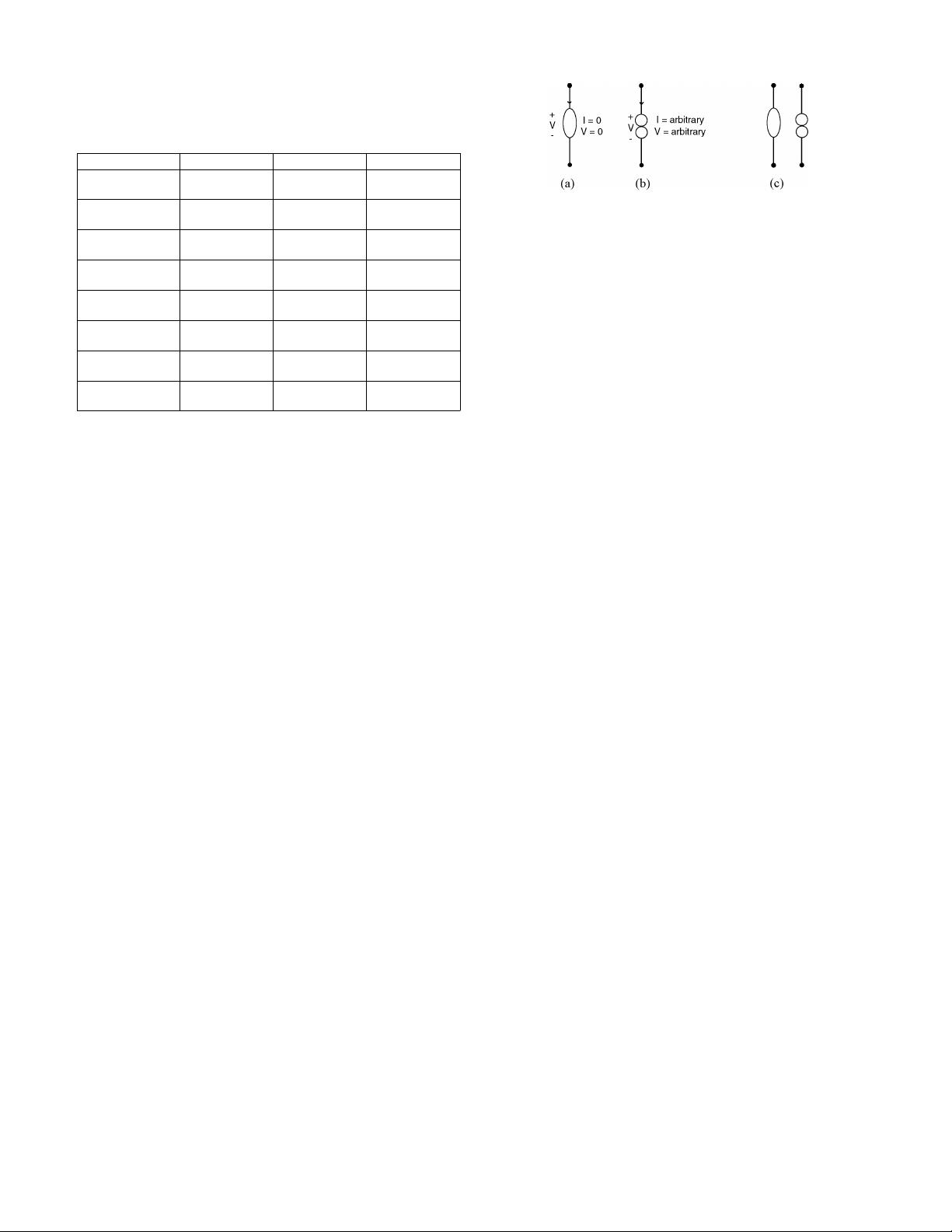
SPICE, and ideal opamps modeled as nullors. A nullor consists
of a nullator and a norator shown in Fig. 3. Nullor is useful
in many linear circuit design problems, such as in switched-
capacitor filters [23]. A major task of this paper is to establish
a set of graph-processing rules for such a set of circuit
elements.
Assumption 1 (Basic Assumption): The following circuit
elements are allowed for GPDD symbolic analysis:
1) linear lumped circuit elements of impedance, ad-
mittance, dependent sources (VCVS, CCCS, VCCS,
CCVS), nullors, and independent sources;
Fig. 3. (a) Nullator. (b) Norator. (c) Nullor.
2) multiple-input multiple-output (MIMO) dependent
sources.
The dependent sources are crucial in linear active circuit
analysis, but treated differently in the traditional symbolic
methods. By modified nodal analysis (MNA), extra current
variables are introduced for the controlled voltage sources
[24]. The well-known two-graph method [25] is based on a
pair of graphs created from the circuit admittance matrix. Its
original formulation does not deal with the non-VCCS-type
dependent sources. The work in [13] introduced type conver-
sions in order to apply the two-graph method for symbolic
analysis. In contrast, the graph-pair method introduced in this
paper processes a pair of graphs directly constructed from
the circuit itself (rather than from its admittance matrix) and
this method can deal with all four types of dependent sources
without the need of type conversion. The work in [26] made
a preliminary contribution to this idea.
A graph-based symbolic analysis method is mainly rule
based. The GPDD method starts from an initial graph that is
created from a given circuit according to several rules. These
rules define the graph edges, the edge directions, and the edge
dependence. We assume for now that a linearized circuit is a
single input and single output. Extension to the MIMO case
is addressed later.
Circuit Graph Construction Rules
1) All dependent source edges are directed; a voltage edge
is directed from the polarity + to − and a current edge
is directed by the given reference direction.
2) An edge is allocated to a controlling voltage (referred to
as VC hereafter) in the graph where the voltage exists. If
one voltage controls m sources (m>1), then m parallel
edges are allocated in the graph where the controlling
voltage exists; each controlling edge is associated with
one controlled source edge.
3) An edge is allocated to a controlling current (referred to
as CC hereafter) in the graph where the current flows.
In case the same current controls m sources (m>1),
then a series of m edges cascaded one after another
are allocated in the graph; each is associated with one
controlled source edge.
4) Any relayed dependent sources are broken up into pair-
wise dependent edges. For example, if edge a controls
edge b, edge b, in turn, controls edge c. Then an extra
edge b
is allocated in parallel to b if b is a voltage (or
in series to b if b is a current) so that edge b
is only
associated with edge c.
5) An ideal opamp is replaced by a pair of nullor edges,
i.e., a nullator edge (referred to as NUL hereafter) and


