This article has been accepted for inclusion in a future issue of this journal. Content is final as presented, with the exception of pagination.
JIANG et al.: 22.3-nW, 4.55 cm
2
TEMPERATURE-ROBUST WURX ACHIEVING A SENSITIVITY OF −69.5 dBm 3
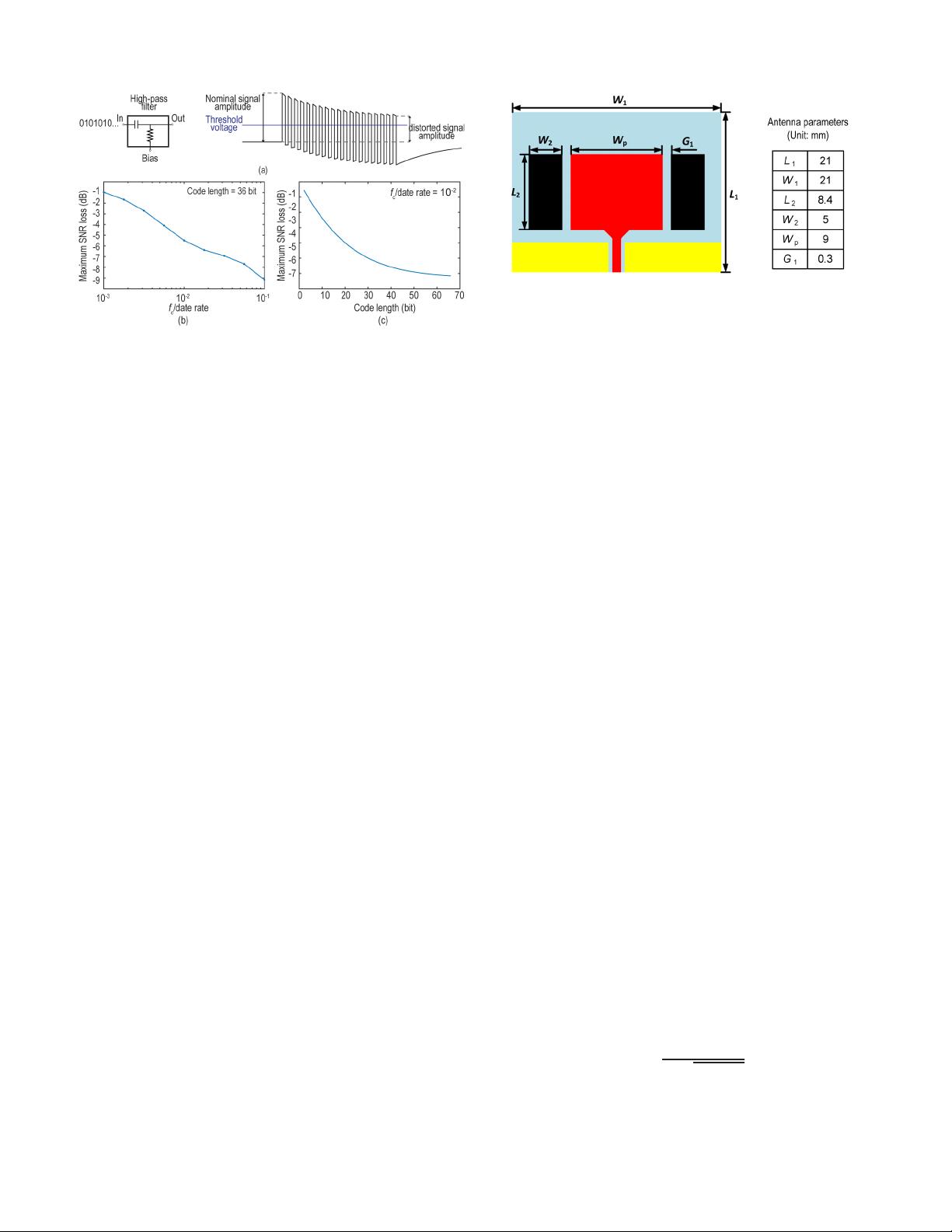
Fig. 3. (a) Simulated waveform output when f
c
/data rate is 0.01 and simu-
lated maximum SNR loss versus (b) f
c
/data rate and (c) code length.
C. BB Circuit Design Challenges
As described in [7], after fixing the architecture and fre-
quency, the only design p arameter that can be traded for
sensitivity is latency. With 20-dBm output power from a
transmitter, better than −65-dBm sensitivity is required to
achieve a reasonable coverage range (∼50 m). To achieve
this sensitivity, a low WuRX data rate (33.3 b/s), a low BB
bandwidth (33.3 Hz), and a long code sequence (18 bit)
are chosen. This results in a latency of 540 ms, which is
acceptable in many, though not all, low-average throughput
IoT applications.
However, the low data rate and the long code sequence
impose a challenge on the conventional ac-coupled BB ampli-
fier [Fig. 1(a)]. Prior work used either nF off-chip capaci-
tors [7] or a 20-pF on-chip capacitor but incurred an SNR
penalty [5]. While the RF components (i.e., antenna and
MN) scale with the carrier frequency, the BB ac-coupling
capacitors are unchanged and only implementable with lumped
components (see Fig. 2).
Fig. 3(a) shows the effect on the signal distortion due to
the ac-coupling. When a signal passes through the high-pass
filter, its dc level shifts toward the bias voltage gradually,
which manifests as a distortion. Since the comparator threshold
voltage is preset to ach ieve the requir ed false-alarm rate and
is constant during the sequence, the signal amplitude with
respect to the threshold voltage decreases with each “1” bit.
The minimum signal amplitude (i.e., the maximum SNR loss)
happens at the end of the last “1” bit. This distortion depends
on the filter corner frequency f
c
and the code (sequence and
length). For example, consider the code consisting of repeating
“10” for simplicity. The maximum SNR loss is plotted against
f
c
normalized to the data rate and code length in Fig. 3(b)
and (c), respectively. The plots show that the distortion is mor e
serious when lower data rates and longer code sequences are
used assuming a fixed f
c
. To bound the distortion to less than
1dB, f
c
must be <0.001× data rate. A similar conclusion
has been drawn in [19, p. 183]. Thus, the 33.3-b/s data rate
needs f
c
≤ 33.3 mHz, which is not possible to reasonably
implement on-chip.
Fig. 4. 9-GHz patch antenna layout.
To address this challenge, dc-coupling should be used
between the ED and BB amplifiers. However, this leads to
issues around biasing (i.e., the preceding stage sets the follow-
ing stage’s operating point) and offset. Section IV proposes an
ED-amplifier co-design scheme where a global CMFB, an AZ
network, and a replica ED are used to address this collectively.
III. RF C
IRCUIT DESIGN
A. Antenna
A patch antenna is a popular choice at high frequency
due to its low cost, high gain, and small form factor that is
compatible with a PCB design. They also have a r elatively nar-
row bandwidth , which is beneficial for interference resilience,
though in some cases, the bandwidth is so narrow that lining
up the antenna’s frequency with the d esired frequency band
and the MN can be difficult. To slightly ease this constraint,
the proposed design employs a conventional patch antenna
next to a pair of parasitic patches, as shown in Fig. 4, which
extends the matching bandwidth from 3% to 5%. The main
patch is 9 × 8.4mm
2
and feeds the following impedance
transformer via a grounded coplanar waveguide (GCPW). The
simulated antenna gain is 5.5 dB.
B. Transformer and Pseudo-Balun ED Co-Design
Prior sub-gigahertz WuRXs utilize discrete components
(inductors and/or MEMS resonators) to implement the MNs
due to their high Q (>100). However, these high-Q passives
become inaccessible as the carrier frequency increases. This
design instead uses distributed components and a bond wire
in the arrangement shown in Fig. 5 to form a transformer. The
T-shaped inductor network (L
1
, L
2
,andL
bond
) is equivalent
to a pair o f coupled inductors. No additional capacitance is
used to avoid extra loss. The ground inductance is carefully
modeled by L
gnd
, as it can significantly affect the performance
at 9 GHz. Specifically, L
gnd
limits the highest operation
frequency since it creates a transmission zero at
f
z,gnd
=
1
2π
L
gnd
C
in
(1)
where C
in
is the ED input capacitance. As shown later, C
in
is
estimated to be 115 fF, and thus, f
z,gnd
should be >15 GHz
so as to not impair the voltage gain at 9 GHz. Thus, L
gnd


