748 CHINESE OPTICS LETTERS / Vol. 6, No. 10 / October 10, 2008
A review of progress on nano-aperture VCSEL
Invited Paper
Zhilong Rao, Sonny Vo, and James S. Harris
Solid State and Photonics Laboratory, Stanford University, Stanford, California, 94305, USA
Received June 18, 2008
This paper reviews the progress on nano-aperture vertical-cavity surface-emitting lasers (VCSELs). The
design, fabrication, and polarization control of nano-aperture VCSELs are reviewed. With the nano-
aperture evolving from conventional circular and square aperture to unique C-shaped, H-shaped, I-shaped,
and bowtie-shaped aperture, both the near-field intensity and near-field beam confinement from nano-
aperture VCSELs are significantly improved. As a high-intensity compact light source with sub-100-
nm spot size, nano-aperture VCSELs are promising to realize many new near-field optical systems and
applications.
OCIS codes: 250.7260, 230.5440, 210.4245.
doi: 10.3788/COL20080610.0748.
1. Introduction
The technological promises of nano-a perture vertical-
cavity surface-emitting lasers (VSCELs) range from
ultrahigh-density near-field optical-data storage to im-
provements in microscopy and ultrahigh-resolution imag-
ing to the study of single molecule manipulation,
fluore scence and spectroscopy, and as a compact light
source for future nanophotonic integrated circuits.
Presently, conventional storage media such as compact
disks, digital video disk, and blue ray disks use far-field
optics. As such, the optical diffraction limit sets an up-
per bound on the optical storage density,
R =
0.61λ
NA
, (1)
where R is the ideal resolution given the wavelength, λ,
and the numerical aperture of the lens system, NA =
n · sin θ
c
.
Partovi et al. first demonstrated the data record-
ing and reading with a 2 50-nm-square-aperture nano-
aperture laser based on a 980-nm wavelength edge emit-
ting laser (EEL). A power output greater than 1 mW
with a small output beam size ranging fr om 50 − 300 nm
were realized. This sugg e sts that recording data with a
density greater than 500 Gb/in
2
will be possible given
better beam confinement and hig her power intensity
[1]
.
VCSELs are better candidates than EEL in these appli-
cations since they can be processed and tested on a wafer
scale. Also, data transfer rates can be greatly increased
by pr oducing VCSELs in linear or two-dimensional (2D)
arrays
[2]
.
Thornton and Hesselink first proposed the idea of
nano-aperture VCSELs
[3]
. To develop a nano-aperture
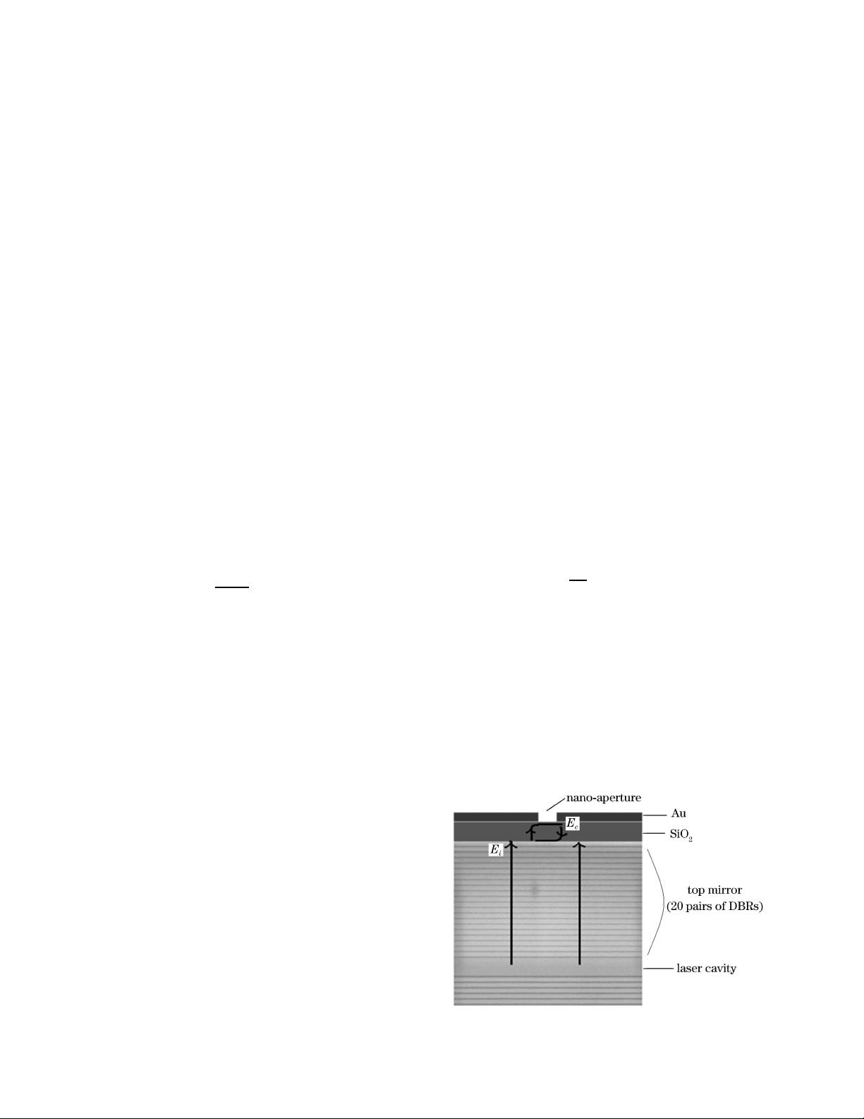
VCSEL, the easiest way is to build it on the foundation
of conventional VCSEL. For example, one c an deposit a
SiO
2
film and then an Au film on top o f a conventional
VCSEL. A nano-aperture VCSEL can be produced by
opening a nano-aperture using a focused ion beam (FIB)
on the Au film. The necessity of using the SiO
2
film
will be discussed later. Figure 1 shows the main part of
the structure of such a nano -aperture VCSEL based on a
conventional VCSEL coated with SiO
2
and a n Au film.
A major short-co ming with this nano-aperture VC-
SEL structure is that the reflectivity of the top mirror
in a conventional VCSEL is very high (typically about
99.5%). As a result, the power output through the top
mirror, namely the intensity of light incident onto the
nano-aperture, is very low compar e d to the intensity in-
side the laser cavity. Thus, the structure of the conven-
tional VCSEL requires revision to increase the output
power.
There a re several possible approaches to improve the
quantum efficiency, and hence, the power output from
the nano-aperture VCSEL, as given by
P
out
=
¯hω
q
η · (I − I
th
), (2)
where ω is the angular lasing frequency, q is the electron
charge, η is the quantum efficiency, I is the injection
current, and I
th
is the lasing threshold current. The first
method, initially proposed by Thornton et al. was to
increase the intensity incident onto the nano-aperture
by reducing the number of distributed Bragg reflecto r
(DBR) pairs in the top mirro r to enhance tr ansmission
[3]
.
The second method was to decr ease the optical mode area
by using a s maller oxide aperture to confine the optical
mode. A third method was to reduce the total loss by
using the oxide aperture to reduce optical scattering loss.
Fig. 1. Schematic structure of nano-aperture VCSEL based
on a conventional VCSEL.
1671-7694/2008/100748-07
c
2008 Chinese Optics Letters


